SLVSE84D December 2017 – July 2021 TLV767
PRODUCTION DATA
- 1 Features
- 2 Applications
- 3 Description
- 4 Revision History
- 5 Pin Configuration and Functions
- 6 Specifications
- 7 Typical Characteristics
- 8 Detailed Description
- 9 Application and Implementation
- 10Power Supply Recommendations
- 11Layout
- 12Device and Documentation Support
5 Pin Configuration and Functions
Figure 5-1 DRV Package (Adjustable), 6-Pin WSON,
Top View
Top View
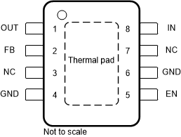
 Figure 5-3 DGN Package (Adjustable),
 8-Pin HVSSOP, Top View
Figure 5-5 DBV Package (Fixed),
5-Pin SOT-23,Top View
5-Pin SOT-23,Top View
Figure 5-2 DRV Package (Fixed), 6-Pin WSON,
Top View
Top View
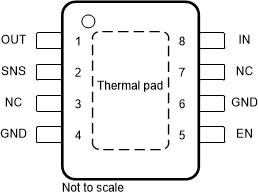
 Figure 5-4 DGN Package (Fixed), 8-Pin HVSSOP, Top View
Table 5-1 Pin Functions
| PIN | I/O | DESCRIPTION | |||||
|---|---|---|---|---|---|---|---|
| NAME | DRV (Adj) |
DRV (Fixed) |
DGN (Adj) |
DGN (Fixed) |
DBV (Fixed) |
||
| EN | 4 | 4 | 5 | 5 | 3 | I | Enable pin. Driving the enable pin high enables the device. Driving this pin low disables the device. High and low thresholds are listed in the Electrical Characteristics table. This pin has an internal pullup and can be left floating to enable the device or the pin can be connected to the input pin. |
| FB | 2 | — | 2 | — | — | I | Feedback pin. Input to the control-loop error amplifier. This pin is used to set the output voltage of the device with the use of external resistors. Do not float this pin. For adjustable-voltage version devices only. |
| GND | 3, 5 | 3, 5 | 4, 6 | 4, 6 | 2 | — | Ground pin. All ground pins must be grounded. |
| DNC | — | — | — | — | 4 | — | Do not connect to a biased voltage. Tie this pin to ground or leave floating |
| IN | 6 | 6 | 8 | 8 | 1 | I | Input pin. Use the recommended capacitor value as listed in the Recommended Operating Conditions table. Place the input capacitor as close to the IN and GND pins of the device as possible. |
| OUT | 1 | 1 | 1 | 1 | 5 | O | Output pin. Use the recommended capacitor value as listed in the Recommended Operating Conditions table. Place the output capacitor as close to the OUT and GND pins of the device as possible. |
| SNS | — | 2 | — | 2 | — | I | Output sense pin. Connect the SNS pin to the OUT pin, or to remotely sense the output voltage at the load, connect the SNS pin to the load. Do not float this pin. For fixed-voltage version devices only. |
| Thermal pad | Pad | Pad | Pad | Pad | — | — | Exposed pad of the package. Connect this pad to ground or leave floating. Connect the thermal pad to a large-area ground plane for best thermal performance. |