SLVSEA2D August 2020 – April 2024 DRV8714-Q1 , DRV8718-Q1
PRODMIX
- 1
- 1 Features
- 2 Applications
- 3 Description
- 4 Device Comparison Table
- 5 Pin Configuration and Functions
- 6 Specifications
-
7 Detailed Description
- 7.1 Overview
- 7.2 Functional Block Diagram
- 7.3
Feature Description
- 7.3.1 External Components
- 7.3.2 Device Interface Variants
- 7.3.3 Input PWM Control Modes
- 7.3.4 Smart Gate Driver
- 7.3.5 Tripler (Dual-Stage) Charge Pump
- 7.3.6 Wide Common-Mode Current Shunt Amplifiers
- 7.3.7 Pin Diagrams
- 7.3.8
Protection and Diagnostics
- 7.3.8.1 Gate Driver Disable (DRVOFF/nFLT and EN_DRV)
- 7.3.8.2 Low IQ Powered Off Braking (POB, BRAKE)
- 7.3.8.3 Fault Reset (CLR_FLT)
- 7.3.8.4 DVDD Logic Supply Power on Reset (DVDD_POR)
- 7.3.8.5 PVDD Supply Undervoltage Monitor (PVDD_UV)
- 7.3.8.6 PVDD Supply Overvoltage Monitor (PVDD_OV)
- 7.3.8.7 VCP Charge Pump Undervoltage Lockout (VCP_UV)
- 7.3.8.8 MOSFET VDS Overcurrent Protection (VDS_OCP)
- 7.3.8.9 Gate Driver Fault (VGS_GDF)
- 7.3.8.10 Thermal Warning (OTW)
- 7.3.8.11 Thermal Shutdown (OTSD)
- 7.3.8.12 Offline Short Circuit and Open Load Detection (OOL and OSC)
- 7.3.8.13 Watchdog Timer
- 7.3.8.14 Fault Detection and Response Summary Table
- 7.4 Device Functional Modes
- 7.5 Programming
- 8 Register Maps
- 9 Application Implementation
- 10Device Documentation and Support
- 11Revision History
- 12Mechanical, Packaging, and Orderable Information
7.5.3.1 SPI Interface for Multiple Slaves in Daisy Chain
The DRV871x-Q1 device can be connected in a daisy chain configuration to save GPIO ports when multiple devices are communicating to the same MCU. Figure 7-34 shows the topology when 3 devices are connected in series with waveforms.
 Figure 7-34 Daisy Chain SPI Operation
The first device in the chain shown above receives data from the master controller in the following format. See SDI1 in Figure 7-34
- 2 bytes of Header
- 3 bytes of Address
- 3 bytes of Data
After the data has been transmitted through the chain, the master controller receives it in the following format. See SDO3 in Figure 7-34
- 3 bytes of Status
- 2 bytes of Header (should be identical to the information controller sent)
- 3 bytes of Report
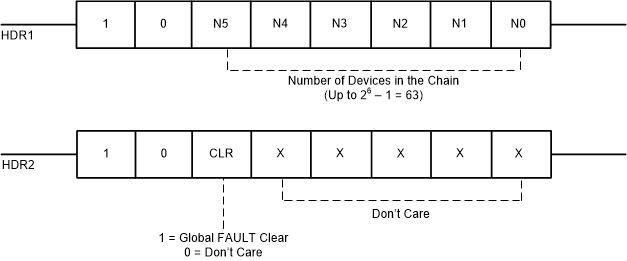
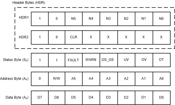
The Header bytes contain information of the number of devices connected in the chain, and a global clear fault command that will clear the fault registers of all the devices on the rising edge of the chip select (nSCS) signal. N5 through N0 are 6 bits dedicated to show the number of device in the chain as shown in Figure 7-35. Up to 63 devices can be connected in series per daisy chain connection.
The 5 LSBs of the HDR2 register are don’t care bits that can be used by the MCU to determine integrity of the daisy chain connection. Header bytes must start with 1 and 0 for the two MSBs.
 Figure 7-35 Header Bits
The Status byte provides information about the fault status register for each device in the daisy chain as shown in Figure 7-36. That way the master controller does not have to initiate a read command to read the fault status from any particular device. This saves the controller additional read commands and makes the system more efficient to determine fault conditions flagged in a device.
 Figure 7-36 Daisy Chain Read Registers
When data passes through a device, it determines the position of itself in the chain by counting the number of Status bytes it receives following by the first Header byte. For example, in this 3 device configuration, device 2 in the chain will receive two Status bytes before receiving HDR1 byte, followed by HDR2 byte.
From the two Status bytes it knows that its position is second in the chain, and from HDR2 byte it knows how many devices are connected in the chain. That way it only loads the relevant address and data byte in its buffer and bypasses the other bits. This protocol allows for faster communication without adding latency to the system for up to 63 devices in the chain.
The address and data bytes remain the same with respect to a single device connection. The Report bytes (R1 through R3), as shown in the figure above, is the content of the register being accessed.