SLVSEI1C June   2019  – October 2020 TPS62864 , TPS62866

PRODUCTION DATA  

  1. Features
  2. Applications
  3. Description
  4. Revision History
  5. Device Options
  6. Pin Configuration and Functions
  7. Specifications
    1. 7.1 Absolute Maximum Ratings
    2. 7.2 ESD Ratings
    3. 7.3 Recommended Operating Conditions
    4. 7.4 Thermal Information
    5. 7.5 Electrical Characteristics
    6. 7.6 I2C InterfaceTiming Characteristics
    7. 7.7 Typical Characteristics
  8. Detailed Description
    1. 8.1 Overview
    2. 8.2 Functional Block Diagram
    3. 8.3 Feature Description
      1. 8.3.1 Power Save Mode
      2. 8.3.2 Forced PWM Mode
      3. 8.3.3 Start-up
      4. 8.3.4 Switch Current Limit and HICCUP Short-Circuit Protection
      5. 8.3.5 Undervoltage Lockout (UVLO)
      6. 8.3.6 Thermal Warning and Shutdown
    4. 8.4 Device Functional Modes
      1. 8.4.1 Enable and Disable (EN)
      2. 8.4.2 Output Discharge
      3. 8.4.3 Start-up Output Voltage and I2C Slave Address Selection (VSET)
      4. 8.4.4 Select Output Voltage Registers (VID)
      5. 8.4.5 Power Good (PG)
    5. 8.5 Programming
      1. 8.5.1 Serial Interface Description
      2. 8.5.2 Standard-, Fast-, and Fast-Mode Plus Protocol
      3. 8.5.3 HS-Mode Protocol
      4. 8.5.4 I2C Update Sequence
      5. 8.5.5 I2C Register Reset
    6. 8.6 Register Map
      1. 8.6.1 Slave Address Byte
      2. 8.6.2 Register Address Byte
      3. 8.6.3 VOUT Register 1
      4. 8.6.4 VOUT Register 2
      5. 8.6.5 CONTROL Register
      6. 8.6.6 STATUS Register
  9. Application and Implementation
    1. 9.1 Application Information
    2. 9.2 Typical Applications
      1. 9.2.1 6-A Output Current Application
        1. 9.2.1.1 Design Requirements
        2. 9.2.1.2 Detailed Design Procedure
          1. 9.2.1.2.1 Custom Design With WEBENCH® Tools
          2. 9.2.1.2.2 Setting The Output Voltage
          3. 9.2.1.2.3 Output Filter Design
          4. 9.2.1.2.4 Inductor Selection
          5. 9.2.1.2.5 Capacitor Selection
        3. 9.2.1.3 Application Curves
      2. 9.2.2 Smaller Application Solution
        1. 9.2.2.1 Design Requirements
        2. 9.2.2.2 Application Curves
  10. 10Power Supply Recommendations
  11. 11Layout
    1. 11.1 Layout Guidelines
    2. 11.2 Layout Example
    3. 11.3 Thermal Considerations
  12. 12Device and Documentation Support
    1. 12.1 Device Support
      1. 12.1.1 Third-Party Products Disclaimer
    2. 12.2 Documentation Support
      1. 12.2.1 Related Documentation
    3. 12.3 Support Resources
    4. 12.4 Receiving Notification of Documentation Updates
    5. 12.5 Trademarks
    6. 12.6 Electrostatic Discharge Caution
    7. 12.7 Glossary
  13. 13Mechanical, Packaging, and Orderable Information
Inductor Selection

The main parameter for the inductor selection is the inductor value and then the saturation current of the inductor. To calculate the maximum inductor current under static load conditions, Equation 2 is given.

Equation 2. GUID-898EF9B2-592F-46F7-A85B-2031B4F56813-low.gif
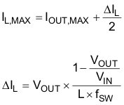
where

  • IOUT,MAX = maximum output current
  • ΔIL = inductor current ripple
  • fSW = switching frequency
  • L = inductor value

It is recommended to choose a saturation current for the inductor that is approximately 20% to 30% higher than IL,MAX. In addition, DC resistance and size must also be taken into account when selecting an appropriate inductor. Table 9-4 lists recommended inductors.

Table 9-4 List of Recommended Inductors
INDUCTANCE [µH]CURRENT RATING, ISAT [A]DIMENSIONS
[L x W x H mm]
DC RESISTANCE [mΩ]PART NUMBER(1)
0.2218.74 x 4 x 25.81Coilcraft, XAL4020-221ME
0.246.62 x 1.6 x 1.213Murata, DFE201612E-R24M
See Third-party Products disclaimer.