SLVSEI2A
November 2018 – May 2019
TPS56339
PRODUCTION DATA.
1
Features
2
Applications
3
Description
Device Images
Simplified Schematic
TPS56339 Efficiency
4
Revision History
5
Pin Configuration and Functions
Pin Functions
6
Specifications
6.1
Absolute Maximum Ratings
6.2
ESD Ratings
6.3
Recommended Operating Conditions
6.4
Thermal Information
6.5
Electrical Characteristics
6.6
Timing Requirements
6.7
Typical Characteristics
7
Detailed Description
7.1
Overview
7.2
Functional Block Diagram
7.3
Feature Description
7.3.1
Advanced Emulated Current Mode Control
7.3.2
Enable and Adjusting Undervoltage Lockout
7.3.3
Soft Start and Pre-Biased Soft Start
7.3.4
Voltage Reference
7.3.5
Minimum ON-time, Minimum OFF-time and Frequency Foldback at Dropout Conditions
7.3.6
Overcurrent and Undervoltage Protection
7.3.7
Thermal Shutdown
7.4
Device Functional Modes
7.4.1
Shutdown Mode
7.4.2
Active Mode
7.4.3
CCM Operation
7.5
Light-Load Operation
8
Application and Implementation
8.1
Application Information
8.2
Typical Application
8.2.1
Design Requirements
8.2.2
Detailed Design Procedure
8.2.2.1
Custom Design With WEBENCH® Tools
8.2.2.2
Output Voltage Resistors Selection
8.2.2.3
Output Inductor Selection
8.2.2.4
Output Capacitor Selection
8.2.2.5
Input Capacitor Selection
8.2.2.6
Bootstrap Capacitor Selection
8.2.3
Undervoltage Lockout Set Point
8.2.4
Application Curves
9
Power Supply Recommendations
10
Layout
10.1
Layout Guidelines
10.2
Layout Example
11
Device and Documentation Support
11.1
Receiving Notification of Documentation Updates
11.2
Related Links
11.3
Community Resources
11.4
Trademarks
11.5
Electrostatic Discharge Caution
11.6
Glossary
12
Mechanical, Packaging, and Orderable Information
8.2.4
Application Curves
V
IN
= 12 V, L
1
= 5.6 µH, C
OUT
= 44 µF, T
A
= 25 °C. (unless otherwise noted)
Figure 18.
Efficiency
Figure 20.
Line Regulation
A.
Figure 22.
Case Temperature Rise vs Load Current
Figure 24.
Steady State Waveforms, I
OUT
= 0.3 A
Figure 26.
Transient Response 1.5 to 3 A
Figure 28.
Startup Relative to V
IN
1.
Figure 30.
Enable Relative to EN
A.
Figure 32.
Short Protection
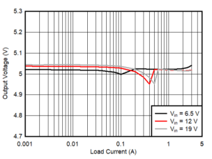
Figure 19.
Load Regulation
Figure 21.
Dropout Curve
Figure 23.
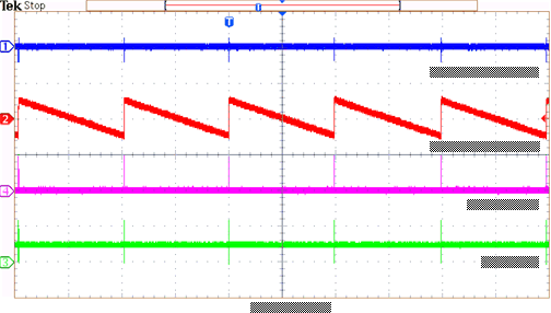
Steady State Waveforms, I
OUT
= 0 A
Figure 25.
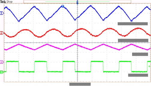
Steady State Waveforms, I
OUT
= 3 A
Figure 27.
Transient Response 0.3 to 2.7 A
Figure 29.
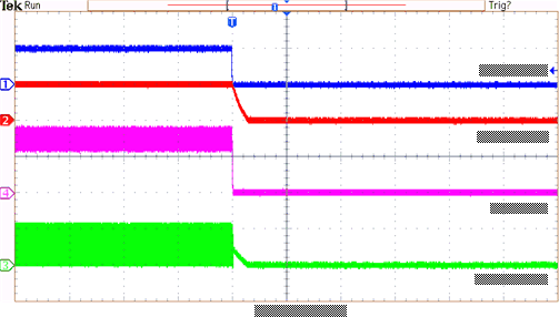
Shutdown Relative to V
IN
1.
Figure 31.
Disable Relative to EN
A.
Figure 33.
Short Recovery