SLVSEK5A August   2018  – October 2018 TPS7B70-Q1

PRODUCTION DATA.  

  1. Features
  2. Applications
  3. Description
    1.     Typical Application
  4. Revision History
  5. Pin Configuration and Functions
    1.     Pin Functions
  6. Specifications
    1. 6.1 Absolute Maximum Ratings
    2. 6.2 ESD Ratings
    3. 6.3 Recommended Operating Conditions
    4. 6.4 Thermal Information
    5. 6.5 Electrical Characteristics
    6. 6.6 Switching Characteristics
    7. 6.7 Typical Characteristics
  7. Detailed Description
    1. 7.1 Overview
    2. 7.2 Functional Block Diagram
    3. 7.3 Feature Description
      1. 7.3.1 Device Enable (EN)
      2. 7.3.2 Adjustable Power-Good Threshold (PG, PGADJ)
      3. 7.3.3 Adjustable Power-Good Delay Timer (DELAY)
      4. 7.3.4 Undervoltage Shutdown
      5. 7.3.5 Current Limit
      6. 7.3.6 Thermal Shutdown
    4. 7.4 Device Functional Modes
      1. 7.4.1 Operation With Input Voltage Less Than 4 V
      2. 7.4.2 Operation With Input Voltage Greater Than 4 V
  8. Application and Implementation
    1. 8.1 Application Information
    2. 8.2 Typical Application
      1. 8.2.1 Design Requirements
      2. 8.2.2 Detailed Design Procedure
        1. 8.2.2.1 Input Capacitor
        2. 8.2.2.2 Output Capacitor
        3. 8.2.2.3 Power-Good Threshold
        4. 8.2.2.4 Power-Good Delay, t(DLY)
      3. 8.2.3 Application Curve
  9. Power Supply Recommendations
  10. 10Layout
    1. 10.1 Layout Guidelines
    2. 10.2 Layout Example
  11. 11Device and Documentation Support
    1. 11.1 Documentation Support
      1. 11.1.1 Related Documentation
    2. 11.2 Receiving Notification of Documentation Updates
    3. 11.3 Community Resources
    4. 11.4 Trademarks
    5. 11.5 Electrostatic Discharge Caution
    6. 11.6 Glossary
  12. 12Mechanical, Packaging, and Orderable Information

Adjustable Power-Good Delay Timer (DELAY)

The power-good delay, t(DLY), is the time from when PGADJ is greater than V(PG,REF) until the PG pin goes high. The power-good delay is a function of the value of the external capacitor that is connected to the DELAY pin (CDELAY). Connecting an external capacitor from this pin to GND sets the power-good delay. The constant current charges an external capacitor until the voltage exceeds a threshold to trip an internal comparator, and Equation 2 determines the power-good delay. Figure 22 illustrates a timing diagram for power-good power-up conditions.

Equation 2. TPS7B70-Q1 eq02-tDLY_SLVSD43.gif

where

  • t(DLY) is the adjustable power-good delay
  • CDELAY is the value of the power-good delay capacitor
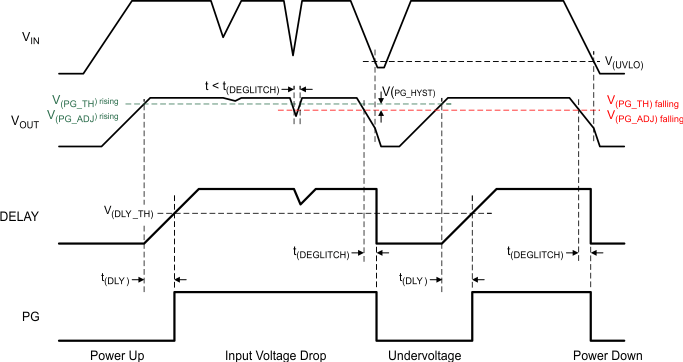
TPS7B70-Q1 pg-activ_SLVSD43.gifFigure 22. Power-Up and Conditions for Activation of Power Good

If the DELAY pin is open, the default delay time is t(DLY_FIX).