SLVSEK5A August 2018 – October 2018 TPS7B70-Q1
PRODUCTION DATA.
- 1 Features
- 2 Applications
- 3 Description
- 4 Revision History
- 5 Pin Configuration and Functions
- 6 Specifications
- 7 Detailed Description
- 8 Application and Implementation
- 9 Power Supply Recommendations
- 10Layout
- 11Device and Documentation Support
- 12Mechanical, Packaging, and Orderable Information
3 Description
The TPS7B70-Q1 is a 300-mA, low-dropout linear regulator (LDO) that operates from an automotive battery. The device has only 19 µA of quiescent current at light loads. Thus, the TPS7B70-Q1 is an excellent selection to supply power to always-on components, such as microcontrollers (MCUs) and controller area network (CAN) transceivers.
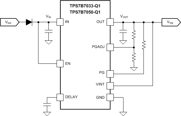
The input voltage range of the TPS7B70-Q1 extends thru 40 V. This voltage helps the device withstand transient conditions, such as load-dump. The device also has a power good (PG) pin to tell the system when the output voltage is in regulation. To achieve the necessary operation, you can adjust the PG threshold voltage and delay. The threshold voltage of the PG signal is adjusted through external resistors. Adjust the delay with an external capacitor.
This device operates in ambient temperatures from –40°C to +125°C, and with junction temperatures from –40°C to +150°C. This device also has a thermally conductive package that enables sustained operation despite significant dissipation across the device, a typical property of off-battery operation. These features, along with included current limit and thermal shutdown protection, make the TPS7B70-Q1 an excellent selection to supply power to automotive system components.
Device Information(1)
| PART NUMBER | OUTPUT VOLTAGE | PACKAGE |
|---|---|---|
| TPS7B70-Q1 | 3.3 V or 5 V | HTSSOP (16) |
- For all available packages, see the package option addendum at the end of the data sheet.
Typical Application
