SLVSEK5A August   2018  – October 2018 TPS7B70-Q1

PRODUCTION DATA.  

  1. Features
  2. Applications
  3. Description
    1.     Typical Application
  4. Revision History
  5. Pin Configuration and Functions
    1.     Pin Functions
  6. Specifications
    1. 6.1 Absolute Maximum Ratings
    2. 6.2 ESD Ratings
    3. 6.3 Recommended Operating Conditions
    4. 6.4 Thermal Information
    5. 6.5 Electrical Characteristics
    6. 6.6 Switching Characteristics
    7. 6.7 Typical Characteristics
  7. Detailed Description
    1. 7.1 Overview
    2. 7.2 Functional Block Diagram
    3. 7.3 Feature Description
      1. 7.3.1 Device Enable (EN)
      2. 7.3.2 Adjustable Power-Good Threshold (PG, PGADJ)
      3. 7.3.3 Adjustable Power-Good Delay Timer (DELAY)
      4. 7.3.4 Undervoltage Shutdown
      5. 7.3.5 Current Limit
      6. 7.3.6 Thermal Shutdown
    4. 7.4 Device Functional Modes
      1. 7.4.1 Operation With Input Voltage Less Than 4 V
      2. 7.4.2 Operation With Input Voltage Greater Than 4 V
  8. Application and Implementation
    1. 8.1 Application Information
    2. 8.2 Typical Application
      1. 8.2.1 Design Requirements
      2. 8.2.2 Detailed Design Procedure
        1. 8.2.2.1 Input Capacitor
        2. 8.2.2.2 Output Capacitor
        3. 8.2.2.3 Power-Good Threshold
        4. 8.2.2.4 Power-Good Delay, t(DLY)
      3. 8.2.3 Application Curve
  9. Power Supply Recommendations
  10. 10Layout
    1. 10.1 Layout Guidelines
    2. 10.2 Layout Example
  11. 11Device and Documentation Support
    1. 11.1 Documentation Support
      1. 11.1.1 Related Documentation
    2. 11.2 Receiving Notification of Documentation Updates
    3. 11.3 Community Resources
    4. 11.4 Trademarks
    5. 11.5 Electrostatic Discharge Caution
    6. 11.6 Glossary
  12. 12Mechanical, Packaging, and Orderable Information

Typical Characteristics

TJ = –40ºC to 150ºC, VIN = 14 V, and VEN ≥ 2 V (unless otherwise noted)
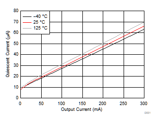
TPS7B70-Q1 D001_SLVSDU9.gif
Figure 1. Ground Current vs Output Current
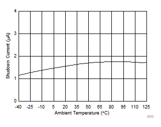
TPS7B70-Q1 D003_SLVSD43.gif
EN = 0 V
Figure 3. Shutdown Current vs Ambient Temperature
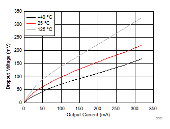
TPS7B70-Q1 D005_SLVSDU9.gif
Figure 5. Dropout Voltage vs Output Current
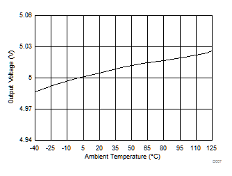
TPS7B70-Q1 D007_SLVSD43.gif
VOUT = 5 V
Figure 7. Output Voltage vs Ambient Temperature
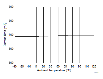
TPS7B70-Q1 D009_SLVSD43.gif
VIN = 5.6 V
Figure 9. Output Current Limit (ILIM) vs Ambient Temperature
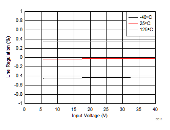
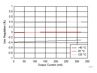
TPS7B70-Q1 D011_SLVSD43.gif
Figure 11. Line Regulation
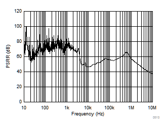
TPS7B70-Q1 D013_SLVSD43.gif
COUT = 10 µF IOUT = 100 mA TA = 25°C
Figure 13. PSRR vs Frequency
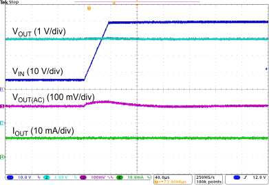
TPS7B70-Q1 D015_SLVSD43.gif
VIN = 6 V to 40 V VOUT = 5 V COUT = 10 µF
IOUT = 1 mA
Figure 15. Line Transient
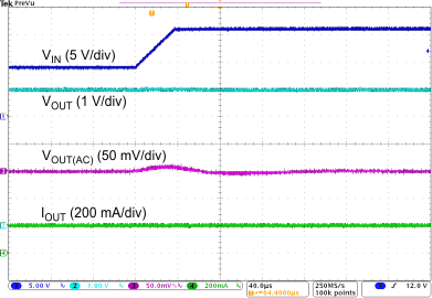
TPS7B70-Q1 D017_SLVSD43.gif
VIN = 6 V to 40 V VOUT = 5 V COUT = 10 µF
IOUT = 200 mA
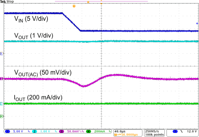
Figure 17. Line Transient
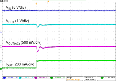
TPS7B70-Q1 D019_SLVSD43.gif
VOUT = 5 V COUT = 10 µF IOUT = 1 mA to 200 mA
Figure 19. Load Transient
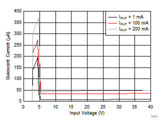
TPS7B70-Q1 D002_SLVSD43.gif
Figure 2. Ground Current vs Input Voltage
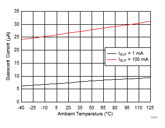
TPS7B70-Q1 D004_SLVSD43.gif
Figure 4. Ground Current vs Ambient Temperature
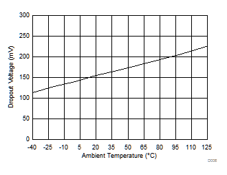
TPS7B70-Q1 D006_SLVSD43.gif
IOUT = 200 mA
Figure 6. Dropout Voltage vs Ambient Temperature
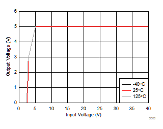
TPS7B70-Q1 D008_SLVSD43.gif
VOUT = 5 V
Figure 8. Output Voltage vs Input Voltage
TPS7B70-Q1 D010_SLVSDU9.gif
Figure 10. Load Regulation
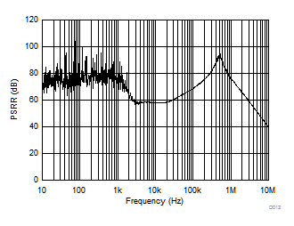
TPS7B70-Q1 D012_SLVSD43.gif
COUT = 10 µF IOUT = 1 mA TA = 25°C
Figure 12. PSRR vs Frequency
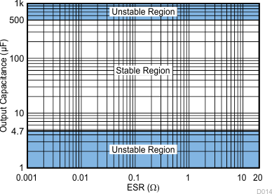
TPS7B70-Q1 D014A_SLVSD43.gif
Figure 14. ESR Stability vs Output Capacitance
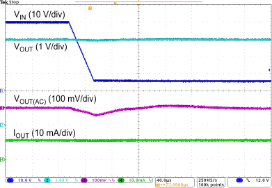
TPS7B70-Q1 D016_SLVSD43.gif
VIN = 40 V to 6 V VOUT = 5 V COUT = 10 µF
IOUT = 1 mA
Figure 16. Line Transient
TPS7B70-Q1 D018_SLVSD43.gif
VIN = 40 V to 6 V VOUT = 5 V COUT = 10 µF
IOUT = 200 mA
Figure 18. Line Transient
TPS7B70-Q1 D020_SLVSD43.gif
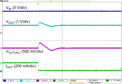
VOUT = 5 V COUT = 10 µF IOUT = 200 mA to 1 mA
Figure 20. Load Transient