SLVSEO1A August 2021 – May 2022 ADC08DJ5200RF
PRODUCTION DATA
- 1 Features
- 2 Applications
- 3 Description
- 4 Revision History
- 5 Pin Configuration and Functions
-
6 Specifications
- 6.1 Absolute Maximum Ratings
- 6.2 ESD Ratings
- 6.3 Recommended Operating Conditions
- 6.4 Thermal Information
- 6.5 Electrical Characteristics: DC Specifications
- 6.6 Electrical Characteristics: Power Consumption
- 6.7 Electrical Characteristics: AC Specifications (Dual-Channel Mode)
- 6.8 Electrical Characteristics: AC Specifications (Single-Channel Mode)
- 6.9 Timing Requirements
- 6.10 Switching Characteristics
- 6.11 Typical Characteristics
-
7 Detailed Description
- 7.1 Overview
- 7.2 Functional Block Diagram
- 7.3
Feature Description
- 7.3.1 Device Comparison
- 7.3.2 Analog Inputs
- 7.3.3 ADC Core
- 7.3.4 Temperature Monitoring Diode
- 7.3.5 Timestamp
- 7.3.6 Clocking
- 7.3.7 Programmable FIR Filter (PFIR)
- 7.3.8
JESD204C Interface
- 7.3.8.1 Transport Layer
- 7.3.8.2 Scrambler
- 7.3.8.3 Link Layer
- 7.3.8.4 8B/10B Link Layer
- 7.3.8.5
64B/66B Link Layer
- 7.3.8.5.1 64B/66B Encoding
- 7.3.8.5.2 Multiblocks, Extended Multiblocks and the Local Extended Multiblock Clock (LEMC)
- 7.3.8.5.3 Block, Multiblock and Extended Multiblock Alignment using Sync Header
- 7.3.8.5.4 Initial Lane Alignment
- 7.3.8.5.5 Block, Multiblock and Extended Multiblock Alignment Monitoring
- 7.3.8.6 Physical Layer
- 7.3.8.7 JESD204C Enable
- 7.3.8.8 Multi-Device Synchronization and Deterministic Latency
- 7.3.8.9 Operation in Subclass 0 Systems
- 7.3.9 Alarm Monitoring
- 7.4
Device Functional Modes
- 7.4.1 Dual-Channel Mode
- 7.4.2 Single-Channel Mode (DES Mode)
- 7.4.3 Dual-Input Single-Channel Mode (DUAL DES Mode)
- 7.4.4 JESD204C Modes
- 7.4.5 Power-Down Modes
- 7.4.6 Test Modes
- 7.4.7 Calibration Modes and Trimming
- 7.4.8 Offset Calibration
- 7.4.9 Trimming
- 7.5 Programming
- 7.6 SPI Register Map
- 8 Application Information Disclaimer
- 9 Power Supply Recommendations
- 10Layout
- 11Device and Documentation Support
- 12Mechanical, Packaging, and Orderable Information
7.3.8.8 Multi-Device Synchronization and Deterministic Latency
JESD204C subclass 1 outlines a method to achieve deterministic latency across the serial link. If two devices achieve the same deterministic latency then they can be considered synchronized. This latency must be achieved from system startup to startup to be deterministic. There are two key requirements to achieve deterministic latency. The first is proper capture of SYSREF for which the device provides a number of features to simplify this requirement at giga-sample clock rates (see the SYSREF Capture section for more information). SYSREF resets either the LMFC in 8B/10B encoding mode or the LEMC is 64B/66B encoding mode. The LMFC and LEMC are analogous between the two modes and are now referred to as LMFC/LEMC.
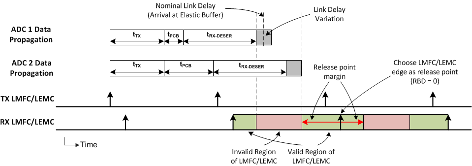
The second requirement is to choose a proper elastic buffer release point in the receiver. Because the device is an ADC, the device is the transmitter (TX) in the JESD204C link and the logic device is the receiver (RX). The elastic buffer is the key block for achieving deterministic latency, and does so by absorbing variations in the propagation delays of the serialized data as the data travels from the transmitter to the receiver. A proper release point is one that provides sufficient margin against delay variations. An incorrect release point results in a latency variation of one LMFC/LEMC period. Choosing a proper release point requires knowing the average arrival time of data at the elastic buffer, referenced to an LMFC/LEMC edge, and the total expected delay variation for all devices. With this information the region of invalid release points within the LMFC/LEMC period can be defined, which stretches from the minimum to maximum delay for all lanes. Essentially, the designer must make sure the data for all lanes arrives at all devices after the previous release point occurs, and before the next release point occurs.
Figure 7-12 provides a timing diagram that demonstrates this requirement. In this figure, the data for two ADCs is shown. The second ADC has a longer routing distance (tPCB) and results in a longer link delay. First, the invalid region of the LMFC/LEMC period is marked off as determined by the data arrival times for all devices. Then, the release point is set by using the release buffer delay (RBD) parameter to shift the release point an appropriate number of frame clocks from the LMFC/LEMC edge so that the release point occurs within the valid region of the LMFC/LEMC cycle. In the case of Figure 7-12, the LMFC/LEMC edge (RBD = 0) is a good choice for the release point because there is sufficient margin on each side of the valid region.
 Figure 7-12 LMFC/LEMC Valid Region Definition for Elastic Buffer Release Point Selection
The TX and RX LMFC/LEMCs do not necessarily need to be phase aligned, but knowledge of their phase is important for proper elastic buffer release point selection. Also, the elastic buffer release point occurs within every LMFC/LEMC cycle, but the buffers only release when all lanes have arrived. Therefore, the total link delay can exceed a single LMFC/LEMC period; see JESD204B multi-device synchronization: Breaking down the requirements for more information.