SLVSEZ5A July 2020 – December 2020 TPS25814
PRODUCTION DATA
- 1 Features
- 2 Applications
- 3 Description
- 4 Revision History
- 5 Pin Configuration and Functions
-
6 Specifications
- 6.1 Absolute Maximum Ratings
- 6.2 ESD Ratings
- 6.3 Recommended Operating Conditions
- 6.4 Recommended Capacitance
- 6.5 Thermal Information
- 6.6 Power Supply Characteristics
- 6.7 Power Consumption
- 6.8 PP_5V Power Switch Characteristics
- 6.9 Power Path Supervisory
- 6.10 CC Cable Detection Parameters
- 6.11 CC VCONN Parameters
- 6.12 Thermal Shutdown Characteristics
- 6.13 Input/Output (I/O) Characteristics
- 6.14 BC1.2 Characteristics
- 6.15 I2C Requirements and Characteristics
- 6.16 Typical Characteristics
- 7 Parameter Measurement Information
-
8 Detailed Description
- 8.1 Overview
- 8.2 Functional Block Diagram
- 8.3 Feature Description
- 8.4 Device Functional Modes
- 9 Application and Implementation
- 10Power Supply Recommendations
- 11Layout
- 12Device and Documentation Support
- 13Mechanical, Packaging, and Orderable Information
8.3.4 Default Behavior Configuration (ADCIN1, ADCIN2)
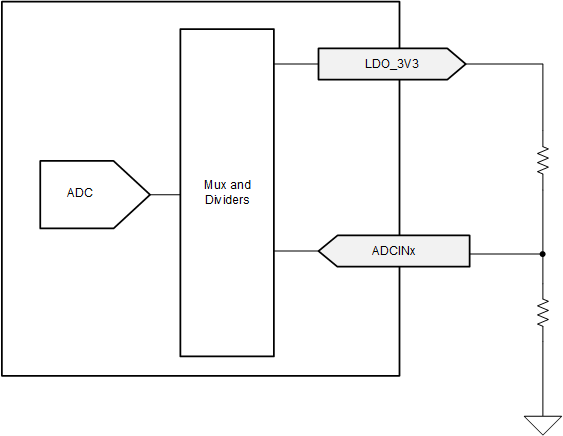
The ADCINx pins must be externally tied to the LDO_3V3 pin via a resistive divider as shown in the following figure. At power-up the ADC converts the ADCINx voltage and the digital core uses these two values to determine the I2C slave address.
 Figure 8-4 ADCINx Resistor Divider
The device behavior is determined in several ways depending upon the decoded value of the ADCIN1 and ADCIN2 pins. The following table shows the decoded values for different resistor divider ratios. See Pin Strapping to Configure Default Behavior for details on how the ADCINx configurations determine default device behavior. See I2C Address Setting for details on how ADCINx decoded values affects default I2C slave address.
| DIV = RDOWN / (RUP + RDOWN) | Without Using RUP or RDOWN | ADCINx Decoded Value | ||||
|---|---|---|---|---|---|---|
| MIN | Target | MAX | ADCINx[2] | ADCINx[1] | ADCINx[0] | |
| 0 | 0.0114 | 0.0228 | tie to GND | 0 | 0 | 0 |
| 0.0229 | 0.0475 | 0.0722 | N/A | 0 | 0 | 1 |
| 0.0723 | 0.1074 | 0.1425 | N/A | 0 | 1 | 0 |
| 0.1425 | 0.1899 | 0.2372 | N/A | 0 | 1 | 1 |
| 0.2373 | 0.3022 | 0.3671 | N/A | 1 | 0 | 0 |
| 0.3672 | 0.5368 | 0.7064 | tie to LDO_1V5 | 1 | 0 | 1 |
| 0.7065 | 0.8062 | 0.9060 | N/A | 1 | 1 | 0 |
| 0.9061 | 0.9530 | 1.0 | tie to LDO_3V3 | 1 | 1 | 1 |