SLVSFE3C November 2020 – December 2021 TPS2661
PRODUCTION DATA
- 1 Features
- 2 Applications
- 3 Description
- 4 Revision History
- 5 Device Comparison Table
- 6 Pin Configuration and Functions
- 7 Specifications
-
8 Detailed Description
- 8.1 Overview
- 8.2 Functional Block Diagram
- 8.3
Feature Description
- 8.3.1 Overload Protection and Fast-Trip
- 8.3.2 Reverse Current Blocking for Unipolar Current Inputs TPS26610, TPS26611 and TPS26612 (4–20 mA, 0–20 mA)
- 8.3.3 OUTPUT and INPUT Cutoff During Overvoltage, Undervoltage Due to Miswiring
- 8.3.4 External Power Supply (±Vs)
- 8.3.5 Loop Testing Without ±Vs Supply (Loop Power Mode in TPS26610, TPS26613 Only)
- 8.3.6 Enable Control With TPS26611, TPS26612, and TPS26614
- 8.3.7 Signal Good Indicator (SGOOD)
- 8.4 Device Functional Modes
-
9 Application and Implementation
- 9.1 Application Information
- 9.2 Typical Application: Analog Input Protection for Current Inputs with TPS26610
- 9.3 Typical Application: Analog Input Protection for Multiplexed Current and Voltage Inputs with TPS26611
- 9.4 System Examples
- 10Power Supply Recommendations
- 11Layout
- 12Device and Documentation Support
- 13Mechanical, Packaging, and Orderable Information
3 Description
The TPS2661x is a compact, feature-rich, fully integrated current loop protector suitable for analog inputs, analog outputs, sensor transmitters, HART inputs, and UART IO protection. The device provides universal input protection for ±20 mA, 0 mA to 20 mA, and 4 mA–20 mA. Low RON values of 7.5 Ω minimizes drop in the current loop, thereby extending operating range and supporting operation even with lower voltage power supplies. The device can withstand and protect the loads from positive and negative supply voltages up to ±50 V. The MODE pin allows flexibility to enable 2x current limit through the device to enable proper start-up of two wire transmitters. Device is capable of operating from an external bipolar supply as low as ± 2.25 V to ±20 V. The device can also be powered from unipolar supplies as low as 3 V to 30 V. The TPS26610 and TPS26613 feature loop power mode to facilitate loop testing in un-powered state without ±Vs supplies.
The device also protects the system from output side miswiring in analog outputs and sensor transmitters by turning off the current path. The internal robust protection control blocks along with the 50-V rating of the TPS2661x help to protect against surge (IEC61000-4-5) and EFT (IEC61000-4-4) transients for signal lines. The device greatly reduces system footprint by its 2.9-mm × 1.6-mm 8-pin SOT-23 package.
| PART NUMBER | PACKAGE | BODY SIZE (NOM) |
|---|---|---|
| TPS26610 | SOT-23 (8) | 2.9 mm × 1.6 mm |
| TPS26611 | ||
| TPS26612 | ||
| TPS26613 | ||
| TPS26614 |
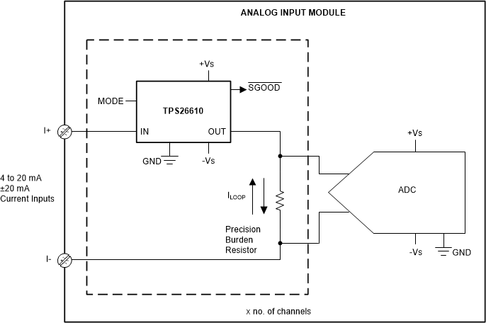
 Typical Circuit Schematic
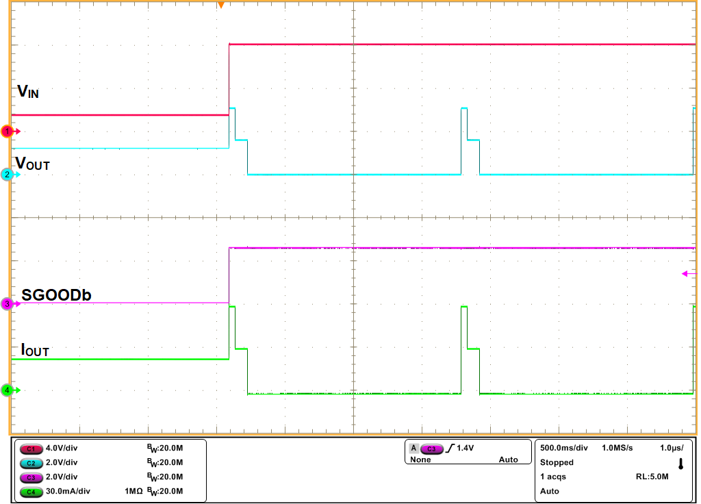
 Miswiring Protection on Input From Field
Supply