SLVSFF0B June   2020  – July 2022 DRV8436E

PRODUCTION DATA  

  1. Features
  2. Applications
  3. Description
  4. Revision History
    1.     Device Options
  5. Pin Configuration and Functions
  6. Specifications
    1. 6.1 Absolute Maximum Ratings
    2. 6.2 ESD Ratings
    3. 6.3 Recommended Operating Conditions
    4. 6.4 Thermal Information
    5. 6.5 Electrical Characteristics
    6. 6.6 Typical Characteristics
  7. Detailed Description
    1. 7.1 Overview
    2. 7.2 Functional Block Diagrams
    3. 7.3 Feature Description
      1. 7.3.1 PWM Motor Drivers
      2. 7.3.2 Bridge Control
      3. 7.3.3 Current Regulation
      4. 7.3.4 Decay Modes
        1. 7.3.4.1 Slow Decay
        2. 7.3.4.2 Mixed Decay
        3. 7.3.4.3 Fast Decay
        4. 7.3.4.4 Smart tune Dynamic Decay
        5. 7.3.4.5 Blanking time
      5. 7.3.5 Charge Pump
      6. 7.3.6 Linear Voltage Regulators
      7. 7.3.7 Logic and Quad-Level Pin Diagrams
        1. 7.3.7.1 nFAULT Pin
      8. 7.3.8 Protection Circuits
        1. 7.3.8.1 VM Undervoltage Lockout (UVLO)
        2. 7.3.8.2 VCP Undervoltage Lockout (CPUV)
        3. 7.3.8.3 Overcurrent Protection (OCP)
        4. 7.3.8.4 Thermal Shutdown (OTSD)
        5. 7.3.8.5 36
    4. 7.4 Device Functional Modes
      1. 7.4.1 Sleep Mode (nSLEEP = 0)
      2. 7.4.2 Operating Mode (nSLEEP = 1)
      3. 7.4.3 Functional Modes Summary
  8. Application and Implementation
    1. 8.1 Application Information
    2. 8.2 Primary Application
      1. 8.2.1 Design Requirements
      2. 8.2.2 Detailed Design Procedure
        1. 8.2.2.1 Current Regulation
    3. 8.3 Typical Application
      1. 8.3.1 Design Requirements
      2. 8.3.2 Detailed Design Procedure
        1. 8.3.2.1 Current Regulation
        2. 8.3.2.2 Stepper Motor Speed
        3. 8.3.2.3 Decay Modes
  9. Power Supply Recommendations
    1. 9.1 Bulk Capacitance
  10. 10Layout
    1. 10.1 Layout Guidelines
    2. 10.2 Layout Example
  11. 11Device and Documentation Support
    1. 11.1 Documentation Support
      1. 11.1.1 Related Documentation
    2. 11.2 Related Links
    3. 11.3 Receiving Notification of Documentation Updates
    4. 11.4 Community Resources
    5. 11.5 Trademarks
  12. 12Mechanical, Packaging, and Orderable Information

Description

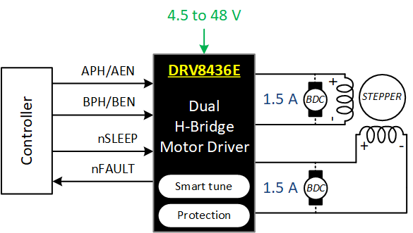
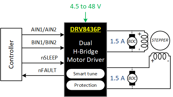
The DRV8436E/P devices are dual H-bridge motor drivers for a wide variety of industrial applications. The devices can be used for driving two DC motors, or a bipolar stepper motor. The output stage of the driver consists of N-channel power MOSFETs configured as two full H-bridges, charge pump regulator, current sensing and regulation, and protection circuitry. The integrated current sensing uses an internal current mirror architecture, removing the need for a large power shunt resistor, saving board area and reducing system cost. A low-power sleep mode is provided to achieve ultra- low quiescent current draw by shutting down most of the internal circuitry. Internal protection features are provided for supply undervoltage lockout (UVLO), charge pump undervoltage (CPUV), output overcurrent (OCP), and device overtemperature (OTSD). The DRV8436E/P is capable of driving up to 1.5-A full scale or 1.1-A rms output current per H-bridge (dependent on PCB design).

Device Information
PART NUMBERPACKAGE(1)BODY SIZE (NOM)
DRV8436EPWPRHTSSOP (28)9.7 mm x 4.4 mm
DRV8436ERGERVQFN (24)4.0 mm x 4.0 mm
DRV8436PPWPRHTSSOP (28)9.7 mm x 4.4 mm
DRV8436PRGERVQFN (24)4.0 mm x 4.0 mm
For all available packages, see the orderable addendum at the end of the data sheet.
GUID-D97419B7-6EA2-49C3-A305-53695DD1E886-low.gifDRV8436E Simplified Schematic
GUID-0E629696-305A-4B98-BB79-0982EA7DBF7E-low.gifDRV8436P Simplified Schematic