SLVSFF0B June 2020 – July 2022 DRV8436E
PRODUCTION DATA
- 1 Features
- 2 Applications
- 3 Description
- 4 Revision History
- 5 Pin Configuration and Functions
- 6 Specifications
- 7 Detailed Description
- 8 Application and Implementation
- 9 Power Supply Recommendations
- 10Layout
- 11Device and Documentation Support
- 12Mechanical, Packaging, and Orderable Information
5 Pin Configuration and Functions
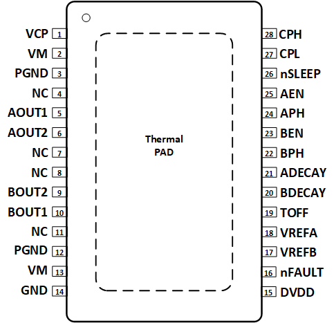
 Figure 5-1 PWP PowerPAD™ Package28-Pin HTSSOPTop View DRV8436E
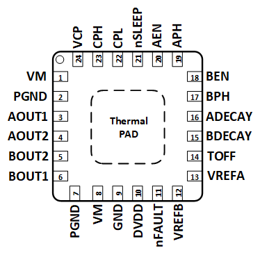
 Figure 5-2 RGE Package24-Pin VQFN with Exposed Thermal PADTop View DRV8436E
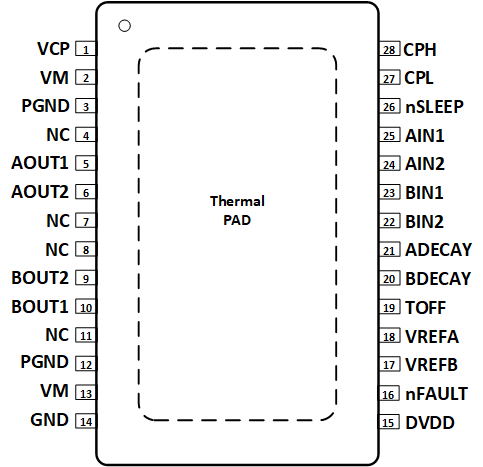
 Figure 5-3 PWP PowerPAD™ Package28-Pin HTSSOPTop View DRV8436P
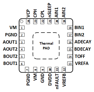
 Figure 5-4 RGE Package24-Pin VQFN with Exposed Thermal PADTop View DRV8436P
Table 5-1 Pin Functions
| PIN | TYPE | DESCRIPTION | ||||
|---|---|---|---|---|---|---|
| NAME | PWP | RGE | ||||
| DRV8436E | DRV8436P | DRV8436E | DRV8436P | |||
| ADECAY | 21 | 21 | 16 | 16 | I | Decay mode setting pins. Set the decay mode for bridge A; quad-level pin. |
| AEN | 25 | — | 20 | — | I | Bridge A enable input. Logic high enables bridge A; logic low disables the bridge Hi-Z. |
| AIN1 | — | 25 | — | 20 | I | Bridge A PWM input. Logic controls the state of H-bridge A; internal pulldown. |
| AIN2 | — | 24 | — | 19 | I | Bridge A PWM input. Logic controls the state of H-bridge A; internal pulldown. |
| AOUT1 | 5 | 5 | 3 | 3 | O | Winding A output. Connect to motor winding. |
| AOUT2 | 6 | 6 | 4 | 4 | O | Winding A output. Connect to motor winding. |
| APH | 24 | — | 19 | — | I | Bridge A phase input. Logic high drives current from AOUT1 to AOUT2. |
| VREFA | 18 | 18 | 13 | 13 | I | Reference voltage input. Voltage on this pin sets the full scale chopping current in H-bridge A. Maximum value 3.3 V. DVDD can be used to provide VREF through a resistor divider. |
| BDECAY | 20 | 20 | 15 | 15 | I | Decay mode setting pins. Set the decay mode for bridge B; quad-level pin. |
| BEN | 23 | — | 18 | — | I | Bridge B enable input. Logic high enables bridge B; logic low disables the bridge Hi-Z. |
| BIN1 | — | 23 | — | 18 | I | Bridge B PWM input. Logic controls the state of H-bridge B; internal pulldown. |
| BIN2 | — | 22 | — | 17 | I | Bridge B PWM input. Logic controls the state of H-bridge B; internal pulldown. |
| BOUT1 | 10 | 10 | 6 | 6 | O | Winding B output. Connect to motor winding. |
| BOUT2 | 9 | 9 | 5 | 5 | O | Winding B output. Connect to motor winding. |
| BPH | 22 | — | 17 | — | I | Bridge B phase input. Logic high drives current from BOUT1 to BOUT2. |
| VREFB | 17 | 17 | 12 | 12 | I | Reference voltage input. Voltage on this pin sets the full scale chopping current in H-bridge B. Maximum value 3.3 V. DVDD can be used to provide VREF through a resistor divider. |
| CPH | 28 | 28 | 23 | 23 | PWR | Charge pump switching node. Connect a X7R, 0.022-μF, VM-rated ceramic capacitor from CPH to CPL. |
| CPL | 27 | 27 | 22 | 22 | ||
| GND | 14 | 14 | 9 | 9 | PWR | Device ground. Connect to system ground. |
| TOFF | 19 | 19 | 14 | 14 | I | Sets the decay mode off-time during current chopping; quad-level pin. |
| DVDD | 15 | 15 | 10 | 10 | PWR | Logic supply voltage. Connect a X7R, 0.47-μF, 6.3-V or 10-V rated ceramic capacitor to GND. |
| VCP | 1 | 1 | 24 | 24 | O | Charge pump output. Connect a X7R, 0.22-μF, 16-V ceramic capacitor to VM. |
| VM | 2, 13 | 2, 13 | 1, 8 | 1, 8 | PWR | Power supply. Connect to motor supply voltage and bypass to GND with two 0.01-μF ceramic capacitors (one for each pin) plus a bulk capacitor rated for VM. |
| PGND | 3, 12 | 3, 12 | 2, 7 | 2, 7 | PWR | Power ground. Both PGND pins are shorted internally. Connect to system ground on PCB. |
| nFAULT | 16 | 16 | 11 | 11 | O | Fault indication. Pulled logic low with fault condition; open-drain output requires an external pullup resistor. |
| nSLEEP | 26 | 26 | 21 | 21 | I | Sleep mode input. Logic high to enable device; logic low to enter low-power sleep mode; internal pulldown resistor. |
| NC | 4, 7, 8, 11 | 4, 7, 8, 11 | - | - | - | No Connect pins. Leave these pins unconnected. |