SLVSFH8B September 2021 – March 2022 LM74720-Q1
PRODUCTION DATA
- 1 Features
- 2 Applications
- 3 Description
- 4 Revision History
- 5 Pin Configuration and Functions
- 6 Specifications
- 7 Parameter Measurement Information
- 8 Detailed Description
-
9 Application and Implementation
- 9.1 Application Information
- 9.2
Typical 12-V Reverse Battery Protection Application
- 9.2.1 Design Requirements for 12-V Battery Protection
- 9.2.2 Automotive Reverse Battery Protection
- 9.2.3
Detailed Design Procedure
- 9.2.3.1 Design Considerations
- 9.2.3.2 Boost Converter Components (C2, C3, L1)
- 9.2.3.3 Input and Output Capacitance
- 9.2.3.4 Hold-Up Capacitance
- 9.2.3.5 Overvoltage Protection and Battery Monitor
- 9.2.3.6 MOSFET Selection: Blocking MOSFET Q1
- 9.2.3.7 MOSFET Selection: Load Disconnect MOSFET Q2
- 9.2.3.8 TVS Selection
- 9.2.4 Application Curves
- 9.3 Do's and Don'ts
- 10Power Supply Recommendations
- 11Layout
- 12Device and Documentation Support
- 13Mechanical, Packaging, and Orderable Information
9.2.2.1 Input Transient Protection: ISO 7637-2 Pulse 1
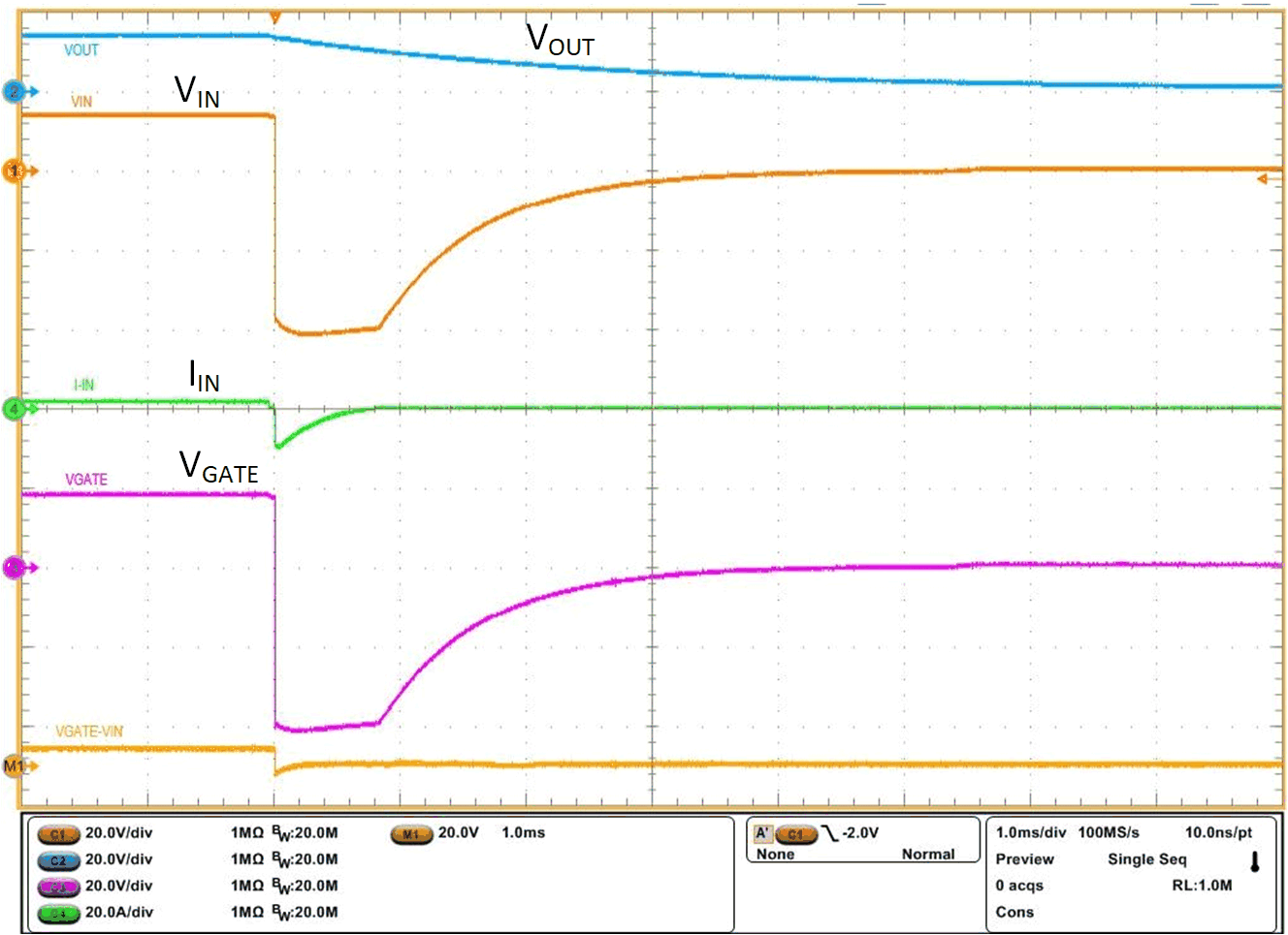
ISO 7637-2 pulse 1 specifies negative transient immunity of electronic modules connected in parallel with an inductive load when the battery is disconnected. A typical pulse 1 specified in ISO 7637-2 starts with battery disconnection where supply voltage collapses to 0 V followed by –150 V 2 ms applied with a source impedance of 10 Ω at a slew rate of 1 µs on the supply input. LM74720-Q1 blocks reverse current and prevents the output voltage from swinging negative, protecting the rest of the electronic circuits from damage due to negative transient voltage. MOSFET Q1 is quickly turned off within 0.5 µs by fast reverse comparator of LM74720-Q1. A single bidirectional TVS is required at the input to clamp the negative transient pulse within the operating maximum voltage across cathode to anode of 85 V and does not violate the MOSFET Q1 drain-source breakdown voltage rating.
Figure 9-2 shows ISO 7637-2 pulse 1 performance of LM74720-Q1.
 Figure 9-2 Performance During ISO 7637-2 Pulse 1 Test