SLVSFJ2B December 2020 – February 2023 TPS22950
PRODUCTION DATA
- 1 Features
- 2 Application
- 3 Description
- 4 Revision History
- 5 Device Comparison Table
- 6 Pin Configuration and Functions
- 7 Specifications
- 8 Parameter Measurement Information
- 9 Detailed Description
- 10Application and Implementation
- 11Device and Documentation Support
- 12Mechanical, Packaging, and Orderable Information
6 Pin Configuration and Functions
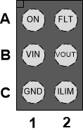
 Figure 6-1 TPS22950xWCSP - 6Top View
Figure 6-2 TPS22950xSOT- 6Top View
Table 6-1 Pin Functions
| PIN | I/O | DESCRIPTION | ||
|---|---|---|---|---|
| NAME | WCSP | SOT6 | ||
| ON | A1 | 1 | I | Active high switch control input. Do not leave floating. |
| FLT | A2 | 6 | O | Open-drain output, pulled low during thermal shutdown or reverse current-conditions. |
| VIN | B1 | 2 | I | Switch input |
| VOUT | B2 | 5 | O | Switch output |
| GND | C1 | 3 | — | Device ground |
| ILIM | C2 | 4 | O | Adjusts device current limit through a resistor to ground. |