SLVSFJ2B December 2020 – February 2023 TPS22950
PRODUCTION DATA
- 1 Features
- 2 Application
- 3 Description
- 4 Revision History
- 5 Device Comparison Table
- 6 Pin Configuration and Functions
- 7 Specifications
- 8 Parameter Measurement Information
- 9 Detailed Description
- 10Application and Implementation
- 11Device and Documentation Support
- 12Mechanical, Packaging, and Orderable Information
3 Description
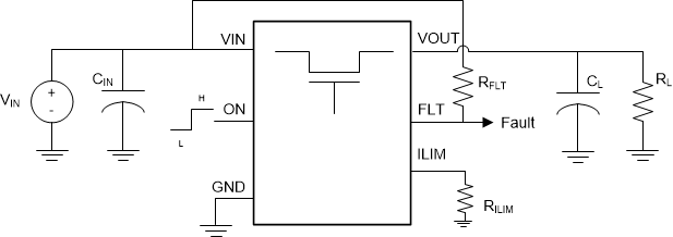
The TPS22950x is a small, single channel load switch with robust protection against fault cases with adjustable output current limiting, reverse current blocking, and thermal shutdown.
The switch ON state is controlled by a digital input that is capable of interfacing directly with low-voltage control signals. When power is first applied, a smart pulldown is used to keep the ON pin from floating until system sequencing is complete. After the pin is deliberately driven high (>VIH), the smart pulldown is disconnected to prevent unnecessary power loss.
The TPS22950/C responds to overcurrent events with auto-retry behavior, while the TPS22950L uses a debounce time and latch off behavior.
TPS22950x is available in a standard WCSP package and leaded SOT package characterized for operation over an ambient temperature range of –40°C to 125°C.
| PART NUMBER | PACKAGE(1) | BODY SIZE (NOM) |
|---|---|---|
| TPS22950, TPS22950L | WCSP (6) | 1.106 mm × 0.706 mm |
| TPS22950C | DDC (SOT, 6) | 2.90 mm × 2.80 mm |
 Typical Application