SLVSFJ9 September 2021 TPS25854-Q1 , TPS25855-Q1
PRODUCTION DATA
- 1 Features
- 2 Applications
- 3 Description
- 4 Revision History
- 5 Description (Continued)
- 6 Device Comparison Table
- 7 Pin Configuration and Functions
- 8 Specifications
- 9 Parameter Measurement Information
-
10Detailed Description
- 10.1 Overview
- 10.2 Functional Block Diagram
- 10.3
Feature Description
- 10.3.1 Power Down or Undervoltage Lockout
- 10.3.2 Input Overvoltage Protection (OVP) - Continuously Monitored
- 10.3.3 Buck Converter
- 10.3.4 FREQ/SYNC
- 10.3.5 Bootstrap Voltage (BOOT)
- 10.3.6 Minimum ON-time, Minimum OFF-time
- 10.3.7 Internal Compensation
- 10.3.8 Current Limit and Short Circuit Protection
- 10.3.9 Cable Compensation
- 10.3.10 Thermal Management With Temperature Sensing (TS) and OTSD
- 10.3.11 Thermal Shutdown
- 10.3.12 FAULT Indication
- 10.3.13 USB Specification Overview
- 10.3.14 USB Type-C® Basics
- 10.3.15 USB Port Operating Modes
- 10.4 Device Functional Modes
-
11Application and Implementation
- 11.1 Application Information
- 11.2
Typical Applications
- 11.2.1 Design Requirements
- 11.2.2
Detailed Design Procedure
- 11.2.2.1 Output Voltage Setting
- 11.2.2.2 Switching Frequency
- 11.2.2.3 Inductor Selection
- 11.2.2.4 Output Capacitor Selection
- 11.2.2.5 Input Capacitor Selection
- 11.2.2.6 Bootstrap Capacitor Selection
- 11.2.2.7 Undervoltage Lockout Set-Point
- 11.2.2.8 Cable Compensation Set-Point
- 11.2.2.9 FAULT, POL, and THERM_WARN Resistor Selection
- 11.2.3 Application Curves
- 12Power Supply Recommendations
- 13Layout
- 14Device and Documentation Support
- 15Mechanical, Packaging, and Orderable Information
10.3.9 Cable Compensation
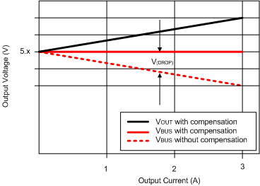
When a load draws current through a long or thin wire, there is an IR drop that reduces the voltage delivered to the load. In the vehicle from the voltage regulator output VOUT to VBUS (input voltage of portable device), the total resistance of PCB trace, connector, and cable resistances causes an IR drop at the portable device input, so the charging current of most portable devices is less than their expected maximum charging current. The voltage drop shows in Figure 10-8.
 Figure 10-8 Voltage Drop
To handle this case, TPS2585x-Q1 builds in the cable compensation function, which increases the voltage at the SENSE pin to compensate the IR drop in the charging path according to the gain set by RIMON, to maintain a fairly constant output voltage at the load-side voltage.
TPS2585x-Q1 use the switch current-sense output voltage to compensate for the line drop voltage. The cable compensation amplitude increases linearly as the load current increases. It also has an upper limit that the maximum cable compensation voltage is 400 mV, the voltage at USB port clamps below 5.5 V. The cable compensation voltage is programmable through an external resistor at IMON pin. RIMON is then chosen by RIMON = ΔVIMON × 1000 / (IBUS × 0.0169), where ΔVOUT is the desired cable droop compensation voltage at full load. See below Table 10-3 and Figure 10-9.
| Resistor at IMON pin | Cable Compensation Voltage at 2.4 A |
|---|---|
| RIMON = 0 Ω | 0 |
| RIMON = 0.976 KΩ | 39.5 mV |
| RIMON = 2.94 KΩ | 119 mV |
| RIMON = 4.99 KΩ | 202 mV |
| RIMON = 6.98 KΩ | 283 mV |
| RIMON = 8.87 KΩ | 360 mV |
| RIMON = 9.76 KΩ | 396 mV |
 Figure 10-9 TPS2585x-Q1 Cable Compensation