SLVSFO5D April 2020 – January 2023 TLV841
PRODUCTION DATA
- 1 Features
- 2 Applications
- 3 Description
- 4 Revision History
- 5 Device Comparison
- 6 Pin Configuration and Functions
- 7 Specifications
- 8 Detailed Description
- 9 Application and Implementation
- 10Power Supply Recommendations
- 11Layout
- 12Device and Documentation Support
- 13Mechanical, Packaging, and Orderable Information
6 Pin Configuration and Functions
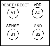
 Figure 6-1 YBH 4-Pin DSBGA Package
(TLV841S)
Top View
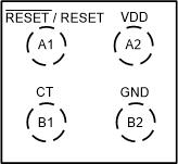
 Figure 6-2 YBH 4-Pin DSBGA Package
(TLV841C)
Top View
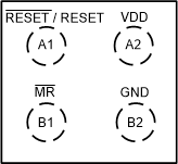
 Figure 6-3 YBH 4-Pin DSBGA Package
 (TLV841M)
Top View
Table 6-1 Pin Functions
| PIN | I/O | DESCRIPTION | |||
|---|---|---|---|---|---|
| PIN NO. | TLV841S | TLV841C | TLV841M | ||
| A1 | RESET | RESET | RESET | O | Active-Low Output Reset Signal for TLV841xxxL: This pin is driven logic low when VDD and SENSE voltage falls below the negative voltage threshold (VIT-) or when the MR voltage falls below the logic low threshold. RESET remains logic low (asserted) until MR is above the logic high threshold or for the duration of the delay time period (tD) after VDD or SENSE voltage rises above VIT- + VHYS |
| A1 | RESET | RESET | RESET | O | Active-High Output Reset Signal for TLV841xxxH: This pin is driven logic high when VDD or SENSE voltage falls below the negative voltage threshold (VIT-) or when the MR voltage falls below the logic low threshold. RESET remains logic high (asserted) until MR is above the logic high threshold or for the duration of the delay time period (tD) after VDD or SENSE voltage rises above VIT- + VHYS |
| A2 | VDD | VDD | VDD | I | Input Supply Voltage: The VDD pin connects to the power supply to power the device. TLV841C and TLV841M monitor VDD voltage. TLV841S monitors SENSE only. Good analog design practice recommends placing a minimum 0.1 µF ceramic capacitor as near as possible to the VDD pin. |
| B1 | SENSE | _ | _ | I | SENSE pin: This pin is connected to the voltage to be monitored. When the voltage on SENSE falls below the negative threshold voltage VIT-, reset asserts. When the voltage on SENSE rises above the positive threshold voltage (VIT- + VHYS), reset deasserts. For noisy applications, placing a 10 nF to 100 nF ceramic capacitor close to this pin may be needed for optimum performance. |
| B1 | _ | CT | _ | I | Capacitor Time Delay Pin: The CT pin offers a user-programmable reset deassert delay time. Connect an external capacitor on this pin to adjust time delay. When not in use leave pin floating for the smallest fixed time delay. |
| B1 | _ | _ | MR | I | Manual Reset: Pull this pin to a logic low to assert a reset signal in the RESET output pin (RESET signal for DL and PL option). After MR pin is left floating or pulls to logic high, the RESET output deasserts to the nominal state after the reset delay time (tD)expires. If unused, the pin can be left floating or connected to VDD. |
| B2 | GND | GND | GND | _ | Ground |