SLVSFP1 August 2021 TPS25868-Q1 , TPS25869-Q1
PRODUCTION DATA
- 1 Features
- 2 Applications
- 3 Description
- 4 Revision History
- 5 Description (continued)
- 6 Device Comparison Table
- 7 Pin Configuration and Functions
- 8 Specifications
- 9 Parameter Measurement Information
-
10Detailed Description
- 10.1 Overview
- 10.2 Functional Block Diagram
- 10.3
Feature Description
- 10.3.1 Power-Down or Undervoltage Lockout
- 10.3.2 Input Overvoltage Protection (OVP) - Continuously Monitored
- 10.3.3 Buck Converter
- 10.3.4 FREQ/SYNC
- 10.3.5 Bootstrap Voltage (BOOT)
- 10.3.6 Minimum ON-Time, Minimum OFF-Time
- 10.3.7 Internal Compensation
- 10.3.8 Selectable Output Voltage (VSET)
- 10.3.9 Current Limit and Short Circuit Protection
- 10.3.10 Cable Compensation
- 10.3.11 Thermal Management with Temperature Sensing (TS) and OTSD
- 10.3.12 Thermal Shutdown
- 10.3.13 USB Enable On/Off Control (TPS25869-Q1)
- 10.3.14 FAULT Indication
- 10.3.15 USB Specification Overview
- 10.3.16 USB Type-C® Basics
- 10.3.17 USB Port Operating Modes
- 10.4 Device Functional Modes
-
11Application and Implementation
- 11.1 Application Information
- 11.2
Typical Applications
- 11.2.1 Design Requirements
- 11.2.2
Detailed Design Procedure
- 11.2.2.1 Output Voltage Setting
- 11.2.2.2 Switching Frequency
- 11.2.2.3 Inductor Selection
- 11.2.2.4 Output Capacitor Selection
- 11.2.2.5 Input Capacitor Selection
- 11.2.2.6 Bootstrap Capacitor Selection
- 11.2.2.7 Undervoltage Lockout Set-Point
- 11.2.2.8 Cable Compensation Set-Point
- 11.2.2.9 FAULT Resistor Selection
- 11.2.3 Application Curves
- 12Power Supply Recommendations
- 13Layout
- 14Device and Documentation Support
- 15Mechanical, Packaging, and Orderable Information
10.3.11 Thermal Management with Temperature Sensing (TS) and OTSD
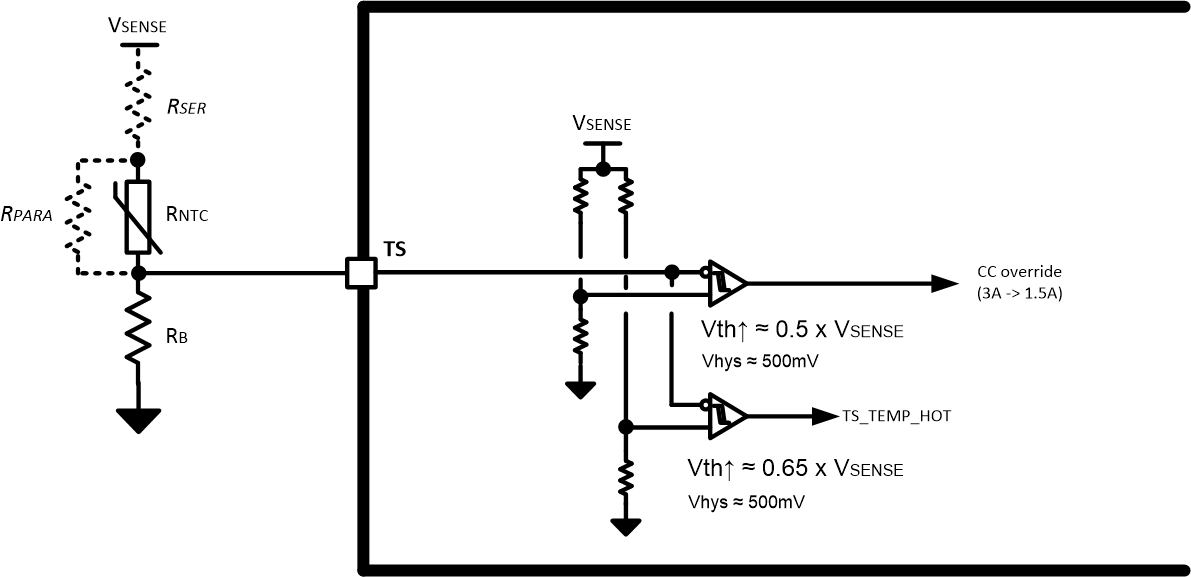
The TS input pin allows for user-programmable thermal protection, see the Electrical Characteristics for the TS pin thresholds. The TS input pin threshold is ratiometric with VSENSE. The external resistor divider setting, VTS, must be connected to the TPS2586x-Q1 SENSE pin to achieve accurate results (refer to the Figure 10-10). When VTS = 0.5 × VSENSE, the TPS2586x-Q1 performs two actions:
- If you are operating with 3-A Type-C advertisement, the PA_CC1, PA_CC2 pin automatically reduces advertisement to the 1.5-A level.
 Figure 10-10 TS Input
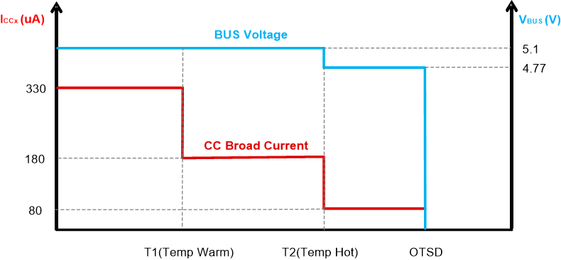
If the overtemperature condition persists, causing VTS = 0.65 × VSENSE, the TPS2586x-Q1 operates at default USB mode, which means it broadcasts the Default USB Power mode, and the output voltage at the SENS pin is reduced to 4.77 V.
In Default USB Power, the charging is ideally reduced further per the USB2.0 and USB3.0 specification.
If the overtemprature condition persists, causing TJ to reach the OTSD threshold, then the device thermal shuts down.
If the overtemprature condition persists, causing TJ to reach the OTSD threshold, then the device thermal shuts down.Figure 10-11 shows the TPS2586x-Q1 behavior when TS pin voltge trigger the Temp Warm and Temp Hot threshold.
 Figure 10-11 TPS2586x-Q1 Behavior When
Trigger Temp Warm and Hot threshold
Figure 10-11 TPS2586x-Q1 Behavior When
Trigger Temp Warm and Hot thresholdThe NTC thermistor must be placed near the hottest point on the PCB. In most cases, this is close to the SW node of the TPS2586x-Q1, near the buck inductor.
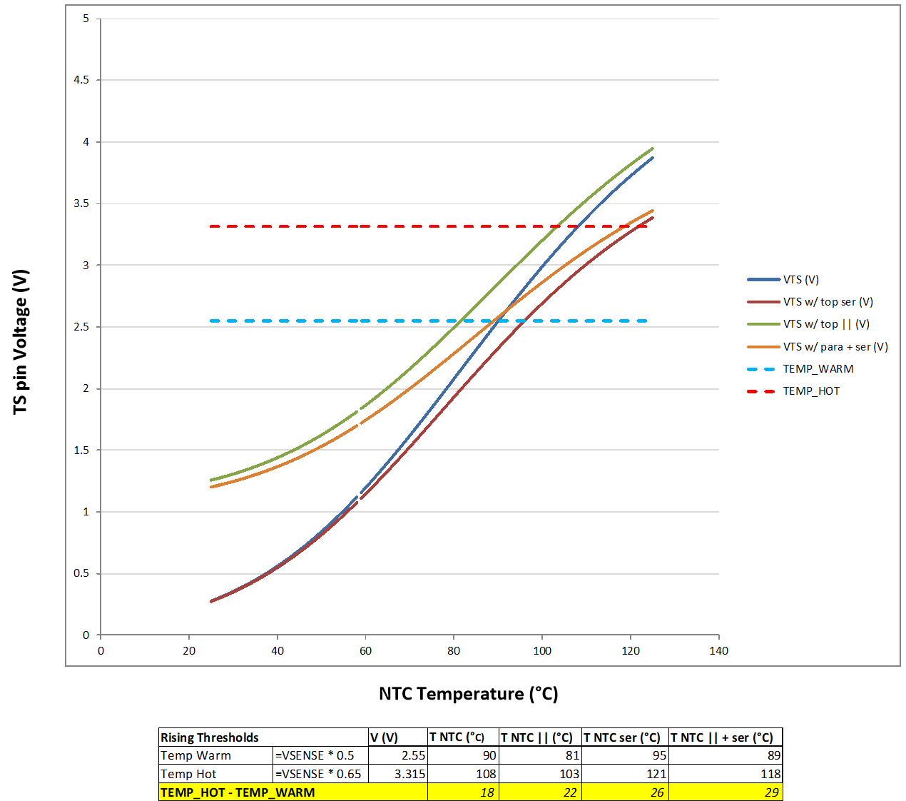
Tuning the VNTC threshold levels of VTEMP_WARM and VTEMP_HOT is achieved by adding RSER, RPARA, or both RSER and RPARA in conjunction with RNTC. Figure 10-12 is an example illustrating how to set the VTEMP_WARM threshold between 81°C and 90°C with a ΔT between TEMP_WARM assertion and TEMP_HOT assertion of 18°C to 29°C. Consult the chosen NTC manufacturer's specification for the value of β. It may take some iteration to establish the desired warning and shutdown thresholds.
Below is NTC spec and resistor value used in Figure 10-12 example.
- R0 = 470 kΩ. β = 4750. RNTC = R0 × exp β × (1/T – 1/T0).
- RPARA = 100 kΩ.
- RSER = 5.1 kΩ.
- RB = RNTC(at TEMP_WARM) = 27 kΩ.
 Figure 10-12 VTS Threshold
Design Examples