SLVSFQ0B October 2020 – June 2024 TPS54J061
PRODUCTION DATA
- 1
- 1 Features
- 2 Applications
- 3 Description
- 4 Pin Configuration and Functions
- 5 Specifications
-
6 Detailed Description
- 6.1 Overview
- 6.2 Functional Block Diagram
- 6.3
Feature Description
- 6.3.1 Enable and Internal LDO
- 6.3.2 Split Rail and External LDO
- 6.3.3 Output Voltage Setting
- 6.3.4 Soft Start and Output-Voltage Tracking
- 6.3.5 Frequency and Operation Mode Selection
- 6.3.6 D-CAP3™ Control Mode
- 6.3.7 Current Sense and Positive Overcurrent Protection
- 6.3.8 Low-side FET Negative Current Limit
- 6.3.9 Power Good
- 6.3.10 Overvoltage and Undervoltage Protection
- 6.3.11 Out-Of-Bounds Operation (OOB)
- 6.3.12 Output Voltage Discharge
- 6.3.13 UVLO Protection
- 6.3.14 Thermal Shutdown
- 6.4 Device Functional Modes
-
7 Application and Implementation
- 7.1 Application Information
- 7.2
Typical Application
- 7.2.1 Design Requirements
- 7.2.2
Detailed Design Procedure
- 7.2.2.1 Choose the Switching Frequency and Operation Mode (MODE Pin)
- 7.2.2.2 Choose the Output Inductor (L)
- 7.2.2.3 Set the Current Limit (TRIP)
- 7.2.2.4 Choose the Output Capacitors (COUT)
- 7.2.2.5 Choose the Input Capacitors (CIN)
- 7.2.2.6 Feedback Network (FB Pin)
- 7.2.2.7 Soft Start Capacitor (SS/REFIN Pin)
- 7.2.2.8 EN Pin Resistor Divider
- 7.2.2.9 VCC Bypass Capacitor
- 7.2.2.10 BOOT Capacitor
- 7.2.2.11 Series BOOT Resistor and RC Snubber
- 7.2.2.12 PGOOD Pullup Resistor
- 7.2.3 Application Curves
- 7.3 Power Supply Recommendations
- 7.4 Layout
- 8 Device and Documentation Support
- 9 Revision History
- 10Mechanical, Packaging, and Ordering Information
3 Description
The TPS54J061 device is a high-efficiency, small-sized, synchronous buck converter with an adaptive on-time D-CAP3 control mode . The device offers ease-of-use and low external-component count for space-conscious power systems.
This device features high-performance integrated MOSFETs, accurate ±1% 600mV reference with an junction temperature range between –40°C and +125°C. Competitive features include very-low external-component count, fast load-transient response, accurate load regulation and line regulation, auto-skip or FCCM mode operation, adjustable soft-start control, and external compensation is not needed to support all ceramic capacitor design .
TPS54J061 is available in a 14-pin QFN package.
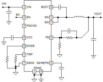
 Simplified Schematic
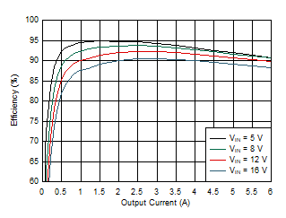
 Typical Efficiency (VOUT = 1.8V, fSW = 600kHz)