SLVSFQ6A November 2020 – June 2021 TPS2640
PRODUCTION DATA
- 1 Features
- 2 Applications
- 3 Description
- 4 Revision History
- 5 Device Comparison
- 6 Pin Configuration and Functions
- 7 Specifications
- 8 Parameter Measurement Information
-
9 Detailed Description
- 9.1 Overview
- 9.2 Functional Block Diagram
- 9.3
Feature Description
- 9.3.1 Undervoltage Lockout (UVLO)
- 9.3.2 Overvoltage Protection (OVP)
- 9.3.3 Reverse Input Supply Protection
- 9.3.4 Hot Plug-In and In-Rush Current Control
- 9.3.5 Overload and Short Circuit Protection
- 9.4 Device Functional Modes
-
10Application and Implementation
- 10.1 Application Information
- 10.2 Typical Application
- 10.3 System Examples
- 10.4 Do's and Dont's
- 11Power Supply Recommendations
- 12Layout
- 13Device and Documentation Support
- 14Mechanical, Packaging, and Orderable Information
10.2.2.4.2 Case 2: Start-Up With Load—Output Capacitance C(OUT) and Load Draws Current During Start-Up
When the load draws current during the turnon sequence, additional power is dissipated in the device. Considering a resistive load RL(SU) during start-up, typical ramp-up of output voltage, load current and the instantaneous power dissipation in the device are shown in Figure 10-4. Instantaneous power dissipation with respect to time is plotted in Figure 10-5. The additional power dissipation during start-up is calculated using Equation 16.

|
VIN = 24 V CdVdT = 2.2 μF |
RL(SU) = 48 Ω COUT = 2.2 mF |
 Due
to Inrush and Load Current")
|
VIN = 24 V CdVdT = 2.2 μF |
RL(SU) = 48 Ω COUT = 2.2 mF |
Total power dissipated in the device during start-up is given by Equation 17.
Total current during start-up is given by Equation 18.
For the design example under discussion,
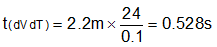
Select the inrush current I(INRUSH) = 0.1 A and calculate tdVdT using Equation 19.
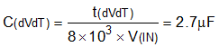
For a given start-up time, CdVdT capacitance value is calculated using Equation 20.
where
- t(dVdT) = 0.528 s
- V(IN) = 24 V
Choose the closest standard value: 2.2-μF/16-V capacitor.
The inrush power dissipation is calculated, using Equation 21.
where
- V(IN) = 24 V
- I(INRUSH) = 0.1 A
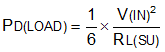
Considering the start-up with 48-Ω load, the additional power dissipation, is calculated using Equation 22.
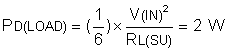
where
- V(IN) = 24 V
- RL(SU) = 48 Ω
The total device power dissipation during start-up is given by Equation 23.
where
- PD(INRUSH) = 1.2 W
- PD(LOAD) = 2 W
The power dissipation with or without load, for a selected start-up time must not exceed the thermal shutdown limits as shown in Figure 10-6 .
From the thermal shutdown limit graph, at TA = 85°C, thermal shutdown time for 3.2 W is close to 28000 ms. It is safe to have a minimum 30% margin to allow for variation of the system parameters such as load, component tolerance, input voltage and layout. Selected 2.2-μF CdVdT capacitor and 528-ms start-up time (tdVdT) are within limit for successful start-up with 48-Ω load.
Higher value C(dVdT) capacitor can be selected to further reduce the power dissipation during start-up.
 Figure 10-6 Thermal Shutdown Time vs Power
Dissipation
Figure 10-6 Thermal Shutdown Time vs Power
Dissipation