SLVSFR1 August 2020 TPS25980
PRODUCTION DATA
- 1 Features
- 2 Applications
- 3 Description
- 4 Revision History
- 5 Device Comparison Table
- 6 Pin Configuration and Functions
- 7 Specifications
-
8 Detailed Description
- 8.1 Overview
- 8.2 Functional Block Diagram
- 8.3 Feature Description
- 8.4 Fault Response
- 8.5 Device Functional Modes
-
9 Application and Implementation
- 9.1 Application Information
- 9.2
Typical Application: Patient Monitoring System in Medical Applications
- 9.2.1 Design Requirements
- 9.2.2
Detailed Design Procedure
- 9.2.2.1 Device Selection
- 9.2.2.2 Setting the Current Limit Threshold: RILIM Selection
- 9.2.2.3 Setting the Undervoltage Lockout Set Point
- 9.2.2.4 Choosing the Current Monitoring Resistor: RIMON
- 9.2.2.5 Setting the Output Voltage Ramp Time (TdVdt)
- 9.2.2.6 Setting the Load Handshake (LDSTRT) Delay
- 9.2.2.7 Setting the Transient Overcurrent Blanking Interval (tITIMER)
- 9.2.2.8 Setting the Auto-Retry Delay and Number of Retries
- 9.2.3 Application Curves
- 9.3 System Examples
- 10Power Supply Recommendations
- 11Layout
- 12Device and Documentation Support
- 13Mechanical, Packaging, and Orderable Information
8.3.6 Power Good (PG)
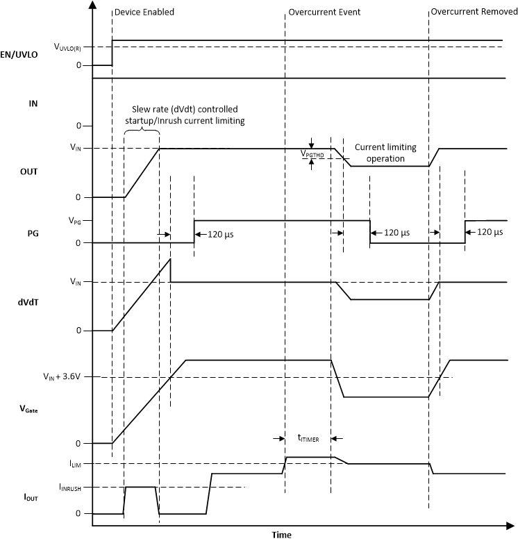
PG is an active high open drain output which indicates whether the FET is fully turned ON and the output voltage has reached the maximum value. After power-up, PG is pulled low initially. The gate driver circuit starts charging the gate capacitance from the internal charge pump. When the FET gate voltage reaches (VIN + 3.6V), PG is asserted after a de-glitch time (tPGD). During normal operation, if at any time VOUT falls below (VIN - VPGTHD), PG is de-asserted after a de-glitch time (tPGD).
 Figure 8-5 Power Good Assertion and De-assertion
1. When there is no supply to the device, the PG pin is expected to stay low. However, there is no active pull-down in this condition to drive this pin all the way down to 0 V. If the PG pin is pulled up to an independent supply which is present even if the TPS25980x is unpowered, there can be a small voltage seen on this pin depending on the pin sink current, which in turn is a function of the pull-up supply voltage and resistor. Minimize the sink current to keep this pin voltage low enough not to be detected as a logic HIGH by associated external circuits in this condition.
2. The PG pin provides a mechanism to detect a possible failed MOSFET condition during start-up. If the PG does not get asserted for an extended period of time after the device is powered up and enabled, it might be an indication of internal MOSFET failure.