SLVSFX8A March 2021 – March 2022 TPS2521
PRODUCTION DATA
- 1 Features
- 2 Applications
- 3 Description
- 4 Revision History
- 5 Device Comparison Table
- 6 Pin Configuration and Functions
- 7 Specifications
-
8 Detailed Description
- 8.1 Overview
- 8.2 Functional Block Diagram
- 8.3
Feature Description
- 8.3.1 Input Reverse Polarity Protection
- 8.3.2 Undervoltage Lockout (UVLO and UVP)
- 8.3.3 Overvoltage Clamp (OVC)
- 8.3.4 Inrush Current, Overcurrent, and Short Circuit Protection
- 8.3.5 Analog Load Current Monitor
- 8.3.6 Reverse Current Protection
- 8.3.7 Overtemperature Protection (OTP)
- 8.3.8 Fault Response
- 8.3.9 Power Good Indication (PG)
- 8.4 Device Functional Modes
- 9 Application and Implementation
- 10Power Supply Recommendations
- 11Layout
- 12Device and Documentation Support
- 13Mechanical, Packaging, and Orderable Information
3 Description
The TPS2521x family of eFuses is a highly integrated circuit protection and power management solution in a small package. The devices provide multiple protection modes using very few external components and are a robust defense against overloads, short-circuits, voltage surges, reverse polarity and excessive inrush current. With integrated back-to-back FETs, reverse current flow from output to input is blocked at all times, making the device well suited for systems which need load side energy hold up storage in case input power supply fails.
Output current limit level can be set with a single external resistor. It is also possible to get an accurate sense of the output load current by measuring the voltage drop across the current limit resistor.
Applications with particular inrush current requirements can set the output slew rate with a single external capacitor. Loads are protected from input overvoltage conditions by clamping the output to a safe fixed maximum voltage (pin selectable).
The devices are available in a 2-mm × 2-mm, 10-pin HotRod QFN package for improved thermal performance and reduced system footprint.
The devices are characterized for operation over a junction temperature range of –40°C to +125°C.
| PART NUMBER | PACKAGE(1) | BODY SIZE (NOM) |
|---|---|---|
| TPS2521xxRPW | QFN (10) | 2 mm × 2 mm |
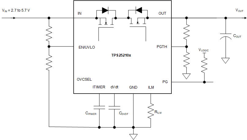
 Simplified Schematic