SLVSGC1B
December 2021 – August 2024
TPS63901
PRODUCTION DATA
1
1
Features
2
Applications
3
Description
4
Pin Configuration and Functions
5
Specifications
5.1
Absolute Maximum Ratings
5.2
ESD Ratings
5.3
Recommended Operating Conditions
5.4
Thermal Information
5.5
Electrical Characteristics
5.6
Typical Characteristics
6
Detailed Description
6.1
Overview
6.2
Functional Block Diagram
6.3
Feature Description
6.3.1
Trapezoidal Current Control
6.3.2
Device Enable and Disable
6.3.3
Soft Start
6.3.4
Input Current Limit
6.3.5
Dynamic Voltage Scaling
6.3.6
Device Configuration (Resistor-to-Digital Interface)
6.3.7
SEL Pin
6.3.8
Short-Circuit Protection
6.3.8.1
Current Limit Setting = 'Unlimited'
6.3.8.2
Current Limit Setting = 1 mA to 100 mA
6.3.9
Thermal Shutdown
6.4
Device Functional Modes
7
Application and Implementation
7.1
Application Information
7.2
Typical Application
7.2.1
Design Requirements
7.2.2
Detailed Design Procedure
7.2.2.1
Inductor Selection
7.2.2.2
Output Capacitor Selection
7.2.2.3
Input Capacitor Selection
7.2.2.4
Setting The Output Voltage
7.2.3
Application Curves
8
Power Supply Recommendations
9
Layout
9.1
Layout Guidelines
9.2
Layout Example
10
Device and Documentation Support
10.1
Device Support
10.1.1
Third-Party Products Disclaimer
10.2
Documentation Support
10.2.1
Related Documentation
10.3
Receiving Notification of Documentation Updates
10.4
Support Resources
10.5
Trademarks
10.6
Electrostatic Discharge Caution
10.7
Glossary
11
Revision History
12
Mechanical, Packaging, and Orderable Information
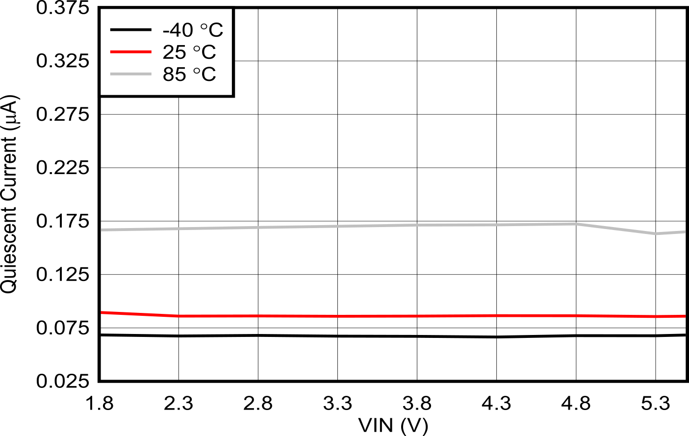
5.6
Typical Characteristics
V
O
= 5.1 V
EN = HIGH
I
O
= 0 mA, device not switching
Figure 5-1
Quiescent Current into VIN vs Input Voltage
V
O
= 5.1 V
EN = LOW
Figure 5-3
Shutdown Current vs Input Voltage
V
O
= 5.1 V
EN = HIGH
I
O
= 0 mA, device not switching
Figure 5-2
Quiescent Current into VOUT vs Input Voltage