SLVSGI0C September   2022  – June 2024 DRV8411

PRODUCTION DATA  

  1.   1
  2. Features
  3. Applications
  4. Description
  5. Device Comparison
  6. Pin Configuration and Functions
  7. Specifications
    1. 6.1 Absolute Maximum Ratings
    2. 6.2 ESD Ratings
    3. 6.3 Recommended Operating Conditions
    4. 6.4 Thermal Information
    5. 6.5 Electrical Characteristics
    6. 6.6 Timing Diagrams
  8. Typical Characteristics
  9. Detailed Description
    1. 8.1 Overview
    2. 8.2 Functional Block Diagram
    3. 8.3 External Components
    4. 8.4 Feature Description
      1. 8.4.1 Bridge Control
        1. 8.4.1.1 Parallel Bridge Interface
      2. 8.4.2 Current Regulation
      3. 8.4.3 Protection Circuits
        1. 8.4.3.1 Overcurrent Protection (OCP)
        2. 8.4.3.2 Thermal Shutdown (TSD)
        3. 8.4.3.3 Undervoltage Lockout (UVLO)
    5. 8.5 Device Functional Modes
      1. 8.5.1 Active Mode
      2. 8.5.2 Low-Power Sleep Mode
      3. 8.5.3 Fault Mode
    6. 8.6 Pin Diagrams
      1. 8.6.1 Logic-Level Inputs
  10. Application and Implementation
    1. 9.1 Application Information
      1. 9.1.1 Typical Application
        1. 9.1.1.1 Stepper Motor Application
          1. 9.1.1.1.1 Design Requirements
          2. 9.1.1.1.2 Detailed Design Procedure
            1. 9.1.1.1.2.1 Stepper Motor Speed
            2. 9.1.1.1.2.2 Current Regulation
            3. 9.1.1.1.2.3 Stepping Modes
              1. 9.1.1.1.2.3.1 Full-Stepping Operation
              2. 9.1.1.1.2.3.2 Half-Stepping Operation with Fast Decay
              3. 9.1.1.1.2.3.3 Half-Stepping Operation with Slow Decay
          3. 9.1.1.1.3 Application Curves
        2. 9.1.1.2 Dual BDC Motor Application
          1. 9.1.1.2.1 Design Requirements
          2. 9.1.1.2.2 Detailed Design Procedure
            1. 9.1.1.2.2.1 Motor Voltage
            2. 9.1.1.2.2.2 Current Regulation
            3. 9.1.1.2.2.3 Sense Resistor
          3. 9.1.1.2.3 Application Curves
        3. 9.1.1.3 Thermal Considerations
          1. 9.1.1.3.1 Maximum Output Current
          2. 9.1.1.3.2 Power Dissipation
          3. 9.1.1.3.3 Thermal Performance
            1. 9.1.1.3.3.1 Steady-State Thermal Performance
            2. 9.1.1.3.3.2 Transient Thermal Performance
        4. 9.1.1.4 Multi-Sourcing with Standard Motor Driver Pinout
    2. 9.2 Power Supply Recommendations
      1. 9.2.1 Bulk Capacitance
      2. 9.2.2 Power Supply and Logic Sequencing
    3. 9.3 Layout
      1. 9.3.1 Layout Guidelines
      2. 9.3.2 Layout Example
  11. 10Device and Documentation Support
    1. 10.1 Documentation Support
      1. 10.1.1 Related Documentation
    2. 10.2 Receiving Notification of Documentation Updates
    3. 10.3 Community Resources
    4. 10.4 Trademarks
  12. 11Revision History
  13. 12Mechanical, Packaging, and Orderable Information

Overcurrent Protection (OCP)

An analog current limit circuit on each FET limits the current through the FET by limiting the gate drive internally. If this current limit persists for longer than the OCP deglitch time (tOCP), all FETs in the H-bridge will disable and the nFAULT pin will assert low. The driver re-enables after the OCP retry period (tRETRY) has passed. nFAULT becomes high again at this time and normal operation resumes. If the fault condition is still present, the cycle repeats as shown in Figure 8-6. Please note that only the H-bridge where an overcurrent condition is detected will be disabled while the other bridge will function normally.
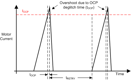
DRV8411 OCP OperationFigure 8-6 OCP Operation

Overcurrent conditions are detected independently on both high- and low-side FETs. This means that a short to ground, supply, or across the motor winding will all result in an overcurrent shutdown. The xISEN pins also integrate a separate overcurrent trip threshold specified by VOCP_ISEN for additional protection when the VM voltage is low or the RSENSE resistance on the xISEN pin is high.