SLVSGI0C September   2022  – June 2024 DRV8411

PRODUCTION DATA  

  1.   1
  2. Features
  3. Applications
  4. Description
  5. Device Comparison
  6. Pin Configuration and Functions
  7. Specifications
    1. 6.1 Absolute Maximum Ratings
    2. 6.2 ESD Ratings
    3. 6.3 Recommended Operating Conditions
    4. 6.4 Thermal Information
    5. 6.5 Electrical Characteristics
    6. 6.6 Timing Diagrams
  8. Typical Characteristics
  9. Detailed Description
    1. 8.1 Overview
    2. 8.2 Functional Block Diagram
    3. 8.3 External Components
    4. 8.4 Feature Description
      1. 8.4.1 Bridge Control
        1. 8.4.1.1 Parallel Bridge Interface
      2. 8.4.2 Current Regulation
      3. 8.4.3 Protection Circuits
        1. 8.4.3.1 Overcurrent Protection (OCP)
        2. 8.4.3.2 Thermal Shutdown (TSD)
        3. 8.4.3.3 Undervoltage Lockout (UVLO)
    5. 8.5 Device Functional Modes
      1. 8.5.1 Active Mode
      2. 8.5.2 Low-Power Sleep Mode
      3. 8.5.3 Fault Mode
    6. 8.6 Pin Diagrams
      1. 8.6.1 Logic-Level Inputs
  10. Application and Implementation
    1. 9.1 Application Information
      1. 9.1.1 Typical Application
        1. 9.1.1.1 Stepper Motor Application
          1. 9.1.1.1.1 Design Requirements
          2. 9.1.1.1.2 Detailed Design Procedure
            1. 9.1.1.1.2.1 Stepper Motor Speed
            2. 9.1.1.1.2.2 Current Regulation
            3. 9.1.1.1.2.3 Stepping Modes
              1. 9.1.1.1.2.3.1 Full-Stepping Operation
              2. 9.1.1.1.2.3.2 Half-Stepping Operation with Fast Decay
              3. 9.1.1.1.2.3.3 Half-Stepping Operation with Slow Decay
          3. 9.1.1.1.3 Application Curves
        2. 9.1.1.2 Dual BDC Motor Application
          1. 9.1.1.2.1 Design Requirements
          2. 9.1.1.2.2 Detailed Design Procedure
            1. 9.1.1.2.2.1 Motor Voltage
            2. 9.1.1.2.2.2 Current Regulation
            3. 9.1.1.2.2.3 Sense Resistor
          3. 9.1.1.2.3 Application Curves
        3. 9.1.1.3 Thermal Considerations
          1. 9.1.1.3.1 Maximum Output Current
          2. 9.1.1.3.2 Power Dissipation
          3. 9.1.1.3.3 Thermal Performance
            1. 9.1.1.3.3.1 Steady-State Thermal Performance
            2. 9.1.1.3.3.2 Transient Thermal Performance
        4. 9.1.1.4 Multi-Sourcing with Standard Motor Driver Pinout
    2. 9.2 Power Supply Recommendations
      1. 9.2.1 Bulk Capacitance
      2. 9.2.2 Power Supply and Logic Sequencing
    3. 9.3 Layout
      1. 9.3.1 Layout Guidelines
      2. 9.3.2 Layout Example
  11. 10Device and Documentation Support
    1. 10.1 Documentation Support
      1. 10.1.1 Related Documentation
    2. 10.2 Receiving Notification of Documentation Updates
    3. 10.3 Community Resources
    4. 10.4 Trademarks
  12. 11Revision History
  13. 12Mechanical, Packaging, and Orderable Information
Application Curves
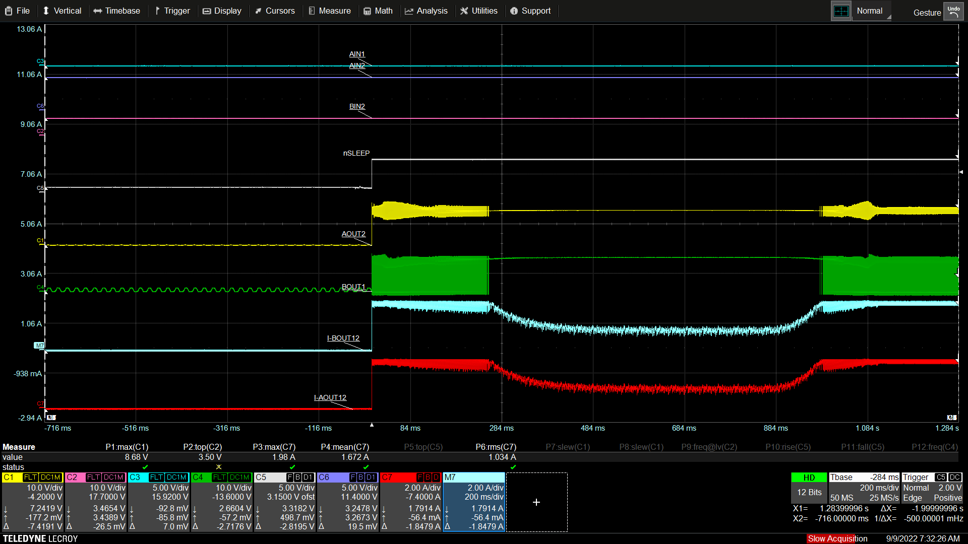
Ch 1 = AOUT2, Ch 2 = BIN2, Ch 3 = AIN1, Ch 4 = BOUT1, Ch 6 = AIN2, Ch 7 = AOUT12 current, Ch M7 = BOUT12 current
DRV8411 No Current RegulationFigure 9-9 No Current Regulation
DRV8411 Current RegulationFigure 9-10 Current Regulation