SLVSGO0 October 2024 TPS25763-Q1
PRODUCTION DATA
- 1
- 1 Features
- 2 Applications
- 3 Description
- 4 Device Comparison Table
- 5 Pin Configuration and Functions
-
6 Specifications
- 6.1 Absolute Maximum Ratings
- 6.2 ESD Ratings
- 6.3 Recommended Operating Conditions
- 6.4 Recommended Components
- 6.5 Thermal Information
- 6.6 Buck-Boost Regulator
- 6.7 CC Cable Detection Parameters
- 6.8 CC VCONN Parameters
- 6.9 CC PHY Parameters
- 6.10 Thermal Shutdown Characteristics
- 6.11 Oscillator Characteristics
- 6.12 ADC Characteristics
- 6.13 TVSP Parameters
- 6.14 Input/Output (I/O) Characteristics
- 6.15 BC1.2 Characteristics
- 6.16 I2C Requirements and Characteristics
- 6.17 Typical Characteristics
- 7 Parameter Measurement Information
-
8 Detailed Description
- 8.1 Overview
- 8.2 Functional Block Diagram
- 8.3
Feature Description
- 8.3.1 Device Power Management and Supervisory Circuitry
- 8.3.2 TVSP Device Configuration and ESD Protection
- 8.3.3 External NFET and LSGD
- 8.3.4
Buck-Boost Regulator
- 8.3.4.1 Buck-Boost Regulator Operation
- 8.3.4.2 Switching Frequency, Frequency Dither, Phase-Shift and Synchronization
- 8.3.4.3 VIN Supply and VIN Over-Voltage Protection
- 8.3.4.4 Feedback Paths and Error Amplifiers
- 8.3.4.5 Transconductors and Compensation
- 8.3.4.6 Output Voltage DAC, Soft-Start and Cable Droop Compensation
- 8.3.4.7 VBUS Overvoltage Protection
- 8.3.4.8 VBUS Undervoltage Protection
- 8.3.4.9 Current Sense Resistor (RSNS) and Current Limit Operation
- 8.3.4.10 Buck-Boost Peak Current Limits
- 8.3.5 USB-PD Physical Layer
- 8.3.6 VCONN
- 8.3.7 Cable Plug and Orientation Detection
- 8.3.8 ADC
- 8.3.9 BC 1.2, Legacy and Fast Charging Modes (Px_DP, Px_DM)
- 8.3.10 DisplayPort Hot-Plug Detect (HPD)
- 8.3.11 USB2.0 Low-Speed Endpoint
- 8.3.12 Digital Interfaces
- 8.3.13 I2C Interface
- 8.3.14 Digital Core
- 8.3.15 NTC Input
- 8.3.16 Thermal Sensors and Thermal Shutdown
- 8.4 Device Functional Modes
- 9 Application and Implementation
- 10Device and Documentation Support
- 11Revision History
- 12Mechanical, Packaging, and Orderable Information
8.3.11 USB2.0 Low-Speed Endpoint
The USB low-speed Endpoint is a USB 2.0 low-speed (1.5 Mbps) interface used to support HID class based accesses. The TPS25763-Q1 supports control of endpoint EP0. This endpoint enumerates to a USB 2.0 host during firmware update mode. Firmware update mode is entered with when the device is powered on with an RTVSP corresponding to TVSP Index 8.
In TPS25763-Q1 devices, the USB Endpoint also provides USB-Billboard information to a host system as defined in the USB Type-C standard. EP0 is used for advertising the Billboard Class. When a Host is connected to a device that provides Alternate Modes which cannot be supported by the Host, the Billboard class allows a means for the Host to report back to the user without any silent failures.
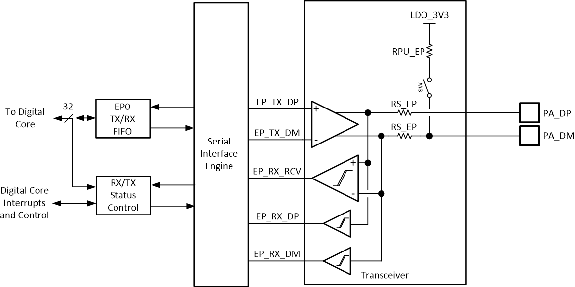
Figure 8-34 shows the USB Endpoint physical layer. The physical layer consists of the analog transceiver, the Serial Interface Engine, and the Endpoint FIFOs and supports low-speed USB operation.
 Figure 8-34 USB Endpoint PHY
The transceiver is made up of a fully differential output driver, a differential to single-ended receive buffer and two single-ended receive buffers on the D+/D– independently. The output driver drives the D+/D– through a source resistance RS_EP. RPU_EP is disconnected during transmit mode of the transceiver.
When the endpoint is in receive mode, the resistance RPU_EP is connected to the PA_DM pin. The RPU_EP resistance advertises low speed mode only.