SLVSGS7D July   2023  – June 2024 TPSM8287A06 , TPSM8287A10 , TPSM8287A12 , TPSM8287A15

PRODUCTION DATA  

  1.   1
  2. Features
  3. Applications
  4. Description
  5. Device Options
  6. Pin Configuration and Functions
  7. Specifications
    1. 6.1 Absolute Maximum Ratings
    2. 6.2 ESD Ratings
    3. 6.3 Recommended Operating Conditions
    4. 6.4 Thermal Information
    5. 6.5 Electrical Characteristics
    6. 6.6 I2C Interface Timing Characteristics
    7. 6.7 Typical Characteristics
  8. Detailed Description
    1. 7.1 Overview
    2. 7.2 Functional Block Diagram
    3. 7.3 Feature Description
      1. 7.3.1  Fixed-Frequency DCS-Control Topology
      2. 7.3.2  Forced-PWM and Power-Save Modes
      3. 7.3.3  Precise Enable
      4. 7.3.4  Start-Up
      5. 7.3.5  Switching Frequency Selection
      6. 7.3.6  Output Voltage Setting
        1. 7.3.6.1 Output Voltage Setpoint
        2. 7.3.6.2 Output Voltage Range
        3. 7.3.6.3 Non-Default Output Voltage Setpoint
        4. 7.3.6.4 Dynamic Voltage Scaling (DVS)
      7. 7.3.7  Compensation (COMP)
      8. 7.3.8  Mode Selection / Clock Synchronization (MODE/SYNC)
      9. 7.3.9  Spread Spectrum Clocking (SSC)
      10. 7.3.10 Output Discharge
      11. 7.3.11 Undervoltage Lockout (UVLO)
      12. 7.3.12 Overvoltage Lockout (OVLO)
      13. 7.3.13 Overcurrent Protection
        1. 7.3.13.1 Cycle-by-Cycle Current Limiting
        2. 7.3.13.2 Hiccup Mode
        3. 7.3.13.3 Current-Limit Mode
      14. 7.3.14 Power Good (PG)
        1. 7.3.14.1 Power-Good Standalone, Primary Device Behavior
        2. 7.3.14.2 Power-Good Secondary Device Behavior
      15. 7.3.15 Remote Sense
      16. 7.3.16 Thermal Warning and Shutdown
      17. 7.3.17 Stacked Operation
    4. 7.4 Device Functional Modes
      1. 7.4.1 Power-On Reset (POR)
      2. 7.4.2 Undervoltage Lockout
      3. 7.4.3 Standby
      4. 7.4.4 On
    5. 7.5 Programming
      1. 7.5.1 Serial Interface Description
      2. 7.5.2 Standard-, Fast-, Fast-Mode Plus Protocol
      3. 7.5.3 I2C Update Sequence
      4. 7.5.4 I2C Register Reset
  9. Device Registers
  10. Application and Implementation
    1. 9.1 Application Information
    2. 9.2 Typical Application
      1. 9.2.1 Design Requirements
      2. 9.2.2 Detailed Design Procedure
        1. 9.2.2.1 Selecting the Input Capacitors
        2. 9.2.2.2 Selecting the Target Loop Bandwidth
        3. 9.2.2.3 Selecting the Compensation Resistor
        4. 9.2.2.4 Selecting the Output Capacitors
        5. 9.2.2.5 Selecting the Compensation Capacitor, CComp1
        6. 9.2.2.6 Selecting the Compensation Capacitor, CComp2
      3. 9.2.3 Application Curves
    3. 9.3 Typical Application Using Four TPSM8287Axx in Parallel Operation
      1. 9.3.1 Design Requirements
      2. 9.3.2 Detailed Design Procedure
        1. 9.3.2.1 Selecting the Input Capacitors
        2. 9.3.2.2 Selecting the Target Loop Bandwidth
        3. 9.3.2.3 Selecting the Compensation Resistor
        4. 9.3.2.4 Selecting the Output Capacitors
        5. 9.3.2.5 Selecting the Compensation Capacitor, CComp1
        6. 9.3.2.6 Selecting the Compensation Capacitor, CComp2
      3. 9.3.3 Application Curves
    4. 9.4 Power Supply Recommendations
    5. 9.5 Layout
      1. 9.5.1 Layout Guidelines
      2. 9.5.2 Layout Example
  11. 10Device and Documentation Support
    1. 10.1 Device Support
      1. 10.1.1 Third-Party Products Disclaimer
    2. 10.2 Documentation Support
      1. 10.2.1 Related Documentation
    3. 10.3 Receiving Notification of Documentation Updates
    4. 10.4 Support Resources
    5. 10.5 Trademarks
    6. 10.6 Electrostatic Discharge Caution
    7. 10.7 Glossary
  12. 11Revision History
  13. 12Mechanical, Packaging, and Orderable Information

Application Curves

VIN = 5.0 V, VOUT = 0.9 V, TA = 25°C, BOM = Table 9-3, unless otherwise noted.

TPSM8287A06 TPSM8287A10 TPSM8287A12 TPSM8287A15 Efficiency TPSM8287A06BAS
VIN = 2.7 VFSW = 1.5 MHzFPWM
Figure 9-2 Efficiency TPSM8287A06BAS
TPSM8287A06 TPSM8287A10 TPSM8287A12 TPSM8287A15 Efficiency TPSM8287A06BAS
VIN = 3.3 V FSW = 1.5 MHz FPWM
Figure 9-4 Efficiency TPSM8287A06BAS
TPSM8287A06 TPSM8287A10 TPSM8287A12 TPSM8287A15 Efficiency TPSM8287A06BAS
VIN = 5.0 V FSW = 1.5 MHz FPWM
Figure 9-6 Efficiency TPSM8287A06BAS
TPSM8287A06 TPSM8287A10 TPSM8287A12 TPSM8287A15 Efficiency TPSM8287A12BAS
VIN = 2.7 VFSW = 1.5 MHz

FPWM

Figure 9-8 Efficiency TPSM8287A12BAS
TPSM8287A06 TPSM8287A10 TPSM8287A12 TPSM8287A15 Efficiency TPSM8287A12BAS
VIN = 3.3 VFSW = 1.5 MHz

FPWM

Figure 9-10 Efficiency TPSM8287A12BAS
TPSM8287A06 TPSM8287A10 TPSM8287A12 TPSM8287A15 Efficiency TPSM8287A12BAS
VIN = 5.0 VFSW = 1.5 MHz

FPWM

Figure 9-12 Efficiency TPSM8287A12BAS
TPSM8287A06 TPSM8287A10 TPSM8287A12 TPSM8287A15 Efficiency TPSM8287A15BAH
VIN = 2.7 VFSW = 1.5 MHz

FPWM

Figure 9-14 Efficiency TPSM8287A15BAH
TPSM8287A06 TPSM8287A10 TPSM8287A12 TPSM8287A15 Efficiency TPSM8287A15BAH
VIN = 3.3 VFSW = 1.5 MHz

FPWM

Figure 9-16 Efficiency TPSM8287A15BAH
TPSM8287A06 TPSM8287A10 TPSM8287A12 TPSM8287A15 Efficiency TPSM8287A15BAH
VIN = 5.0 VFSW = 1.5 MHz

FPWM

Figure 9-18 Efficiency TPSM8287A15BAH
TPSM8287A06 TPSM8287A10 TPSM8287A12 TPSM8287A15 Load Regulation TPSM8287A12BAS
VIN = 2.7 V

TJ = 25 °C

FPWM

Figure 9-20 Load Regulation TPSM8287A12BAS
TPSM8287A06 TPSM8287A10 TPSM8287A12 TPSM8287A15 Load Regulation TPSM8287A12BAS
VIN = 3.3 V

TJ = 25 °C

FPWM

Figure 9-22 Load Regulation TPSM8287A12BAS
TPSM8287A06 TPSM8287A10 TPSM8287A12 TPSM8287A15 Load Regulation TPSM8287A12BAS
VIN = 5.0 V

TJ = 25 °C

FPWM

Figure 9-24 Load Regulation TPSM8287A12BAS
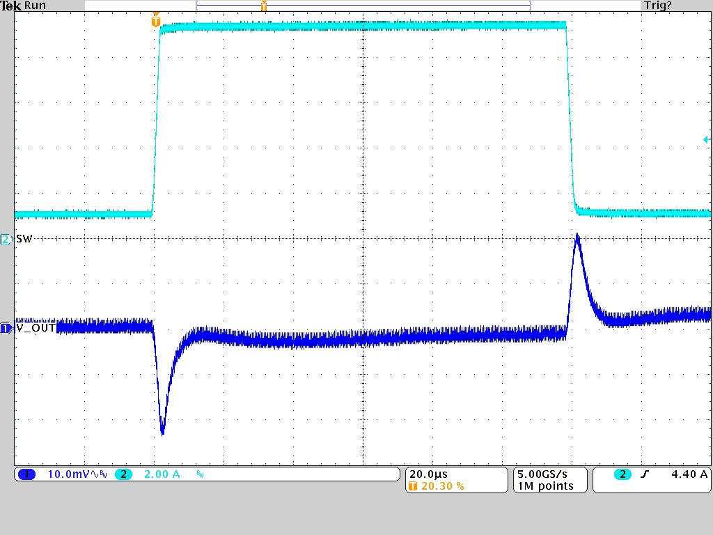
TPSM8287A06 TPSM8287A10 TPSM8287A12 TPSM8287A15 Load Transient Response TPSM8287A12BBS

Vout = 0.9 V

Iout = 1 A → 9 A → 1 A

Figure 9-26 Load Transient Response TPSM8287A12BBS
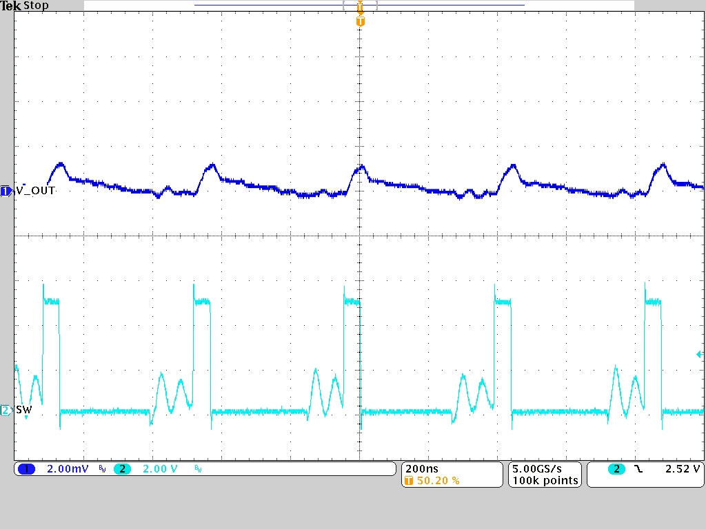
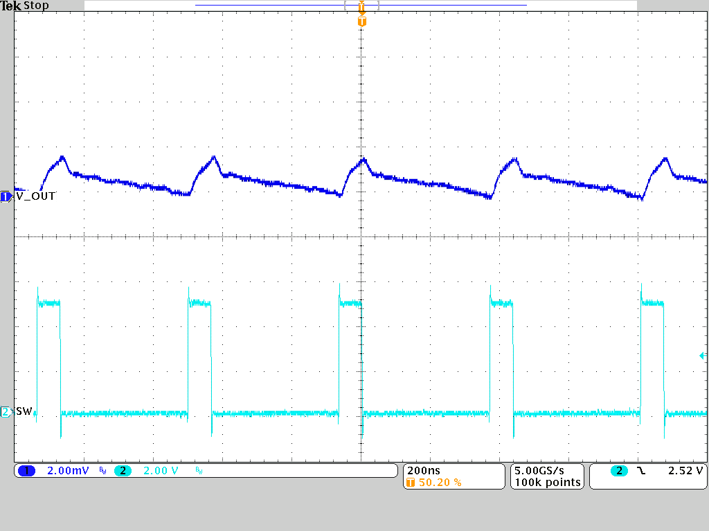
TPSM8287A06 TPSM8287A10 TPSM8287A12 TPSM8287A15 PWM-DCM Operation TPSM8287A12BBS
Vout = 0.9 VIOUT = 1 A
Figure 9-28 PWM-DCM Operation TPSM8287A12BBS
TPSM8287A06 TPSM8287A10 TPSM8287A12 TPSM8287A15 Output Noise over Frequency TPSM8287A12BBS
VIN = 3.3 VVOUT = 0.75 VIOUT = 6 A
Figure 9-30 Output Noise over Frequency TPSM8287A12BBS
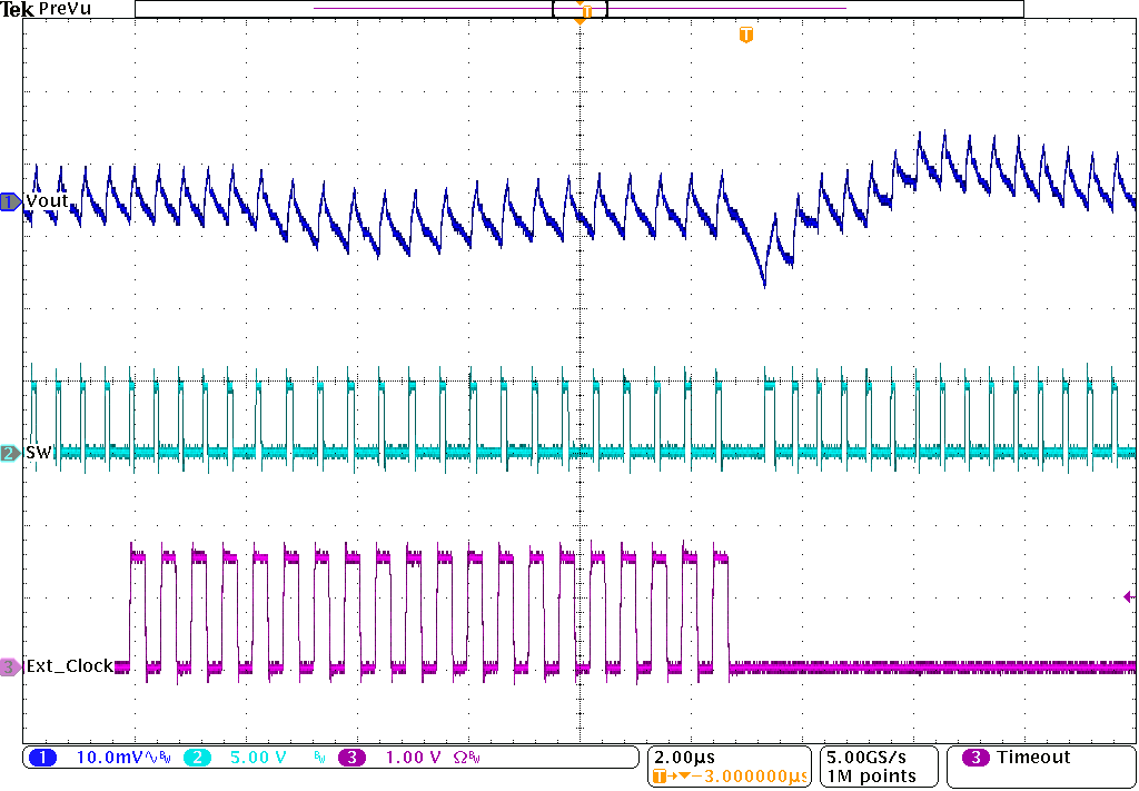
TPSM8287A06 TPSM8287A10 TPSM8287A12 TPSM8287A15 Adding and Removing an External Clock

IOUT = 10 A

VOUT = 0.9 Vf(SYNC) = 1.8 MHz
Figure 9-32 Adding and Removing an External Clock
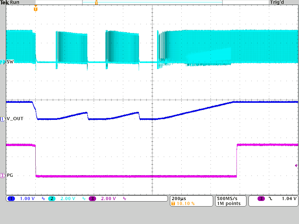
TPSM8287A06 TPSM8287A10 TPSM8287A12 TPSM8287A15 Current Limit (Hiccup)
VIN = 3.3 V
Figure 9-34 Current Limit (Hiccup)
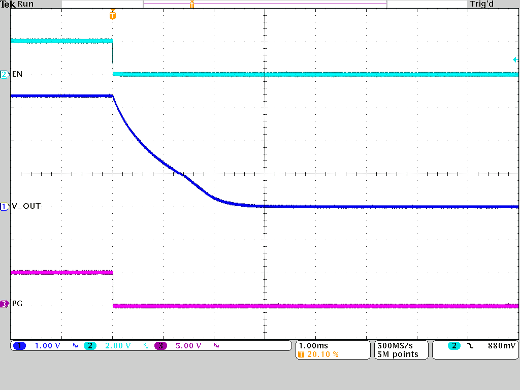
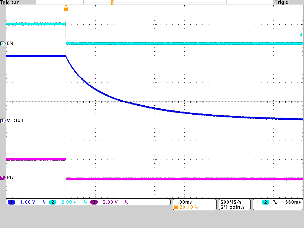
TPSM8287A06 TPSM8287A10 TPSM8287A12 TPSM8287A15 Shutdown Using EN Pin (Discharge Enabled)

VOUT = 3.3 V

Load = 7.5 Ω
Figure 9-36 Shutdown Using EN Pin (Discharge Enabled)
TPSM8287A06 TPSM8287A10 TPSM8287A12 TPSM8287A15 Safe Operating Area TPSM8287A06BAS VIN = 3.3 V

RΘJA = 19.5 °C/W

nat. convection

TJ,max = 125 °C

Figure 9-38 Safe Operating Area TPSM8287A06BAS VIN = 3.3 V
TPSM8287A06 TPSM8287A10 TPSM8287A12 TPSM8287A15 Safe Operating Area TPSM8287A10BAH VIN = 3.3 V

RΘJA = 20.0 °C/W

nat. convection

TJ,max = 125 °C

Figure 9-40 Safe Operating Area TPSM8287A10BAH VIN = 3.3 V
TPSM8287A06 TPSM8287A10 TPSM8287A12 TPSM8287A15 Safe Operating Area TPSM8287A12BAS VIN = 3.3 V

RΘJA = 19.5 °C/W

nat. convection

TJ,max = 125 °C

Figure 9-42 Safe Operating Area TPSM8287A12BAS VIN = 3.3 V
TPSM8287A06 TPSM8287A10 TPSM8287A12 TPSM8287A15 Safe Operating Area TPSM8287A12BBS VIN = 3.3 V
RΘJA = 19.5 °C/Wnat. convectionTJ,max = 125 °C
Figure 9-44 Safe Operating Area TPSM8287A12BBS VIN = 3.3 V
TPSM8287A06 TPSM8287A10 TPSM8287A12 TPSM8287A15 Safe Operating Area TPSM8287A15BAH VIN = 3.3 V
RΘJA = 20.0 °C/Wnat. convectionTJ,max = 125 °C
Figure 9-46 Safe Operating Area TPSM8287A15BAH VIN = 3.3 V
TPSM8287A06 TPSM8287A10 TPSM8287A12 TPSM8287A15 Safe Operating Area TPSM8287A15BBH VIN = 3.3 V
RΘJA = 20.0 °C/Wnat. convectionTJ,max = 125 °C
Figure 9-48 Safe Operating Area TPSM8287A15BBH VIN = 3.3 V
TPSM8287A06 TPSM8287A10 TPSM8287A12 TPSM8287A15 Efficiency TPSM8287A10BAH
VIN = 2.7 V FSW = 1.5 MHz FPWM
Figure 9-3 Efficiency TPSM8287A10BAH
TPSM8287A06 TPSM8287A10 TPSM8287A12 TPSM8287A15 Efficiency TPSM8287A10BAH
VIN = 3.3 V FSW = 1.5 MHz FPWM
Figure 9-5 Efficiency TPSM8287A10BAH
TPSM8287A06 TPSM8287A10 TPSM8287A12 TPSM8287A15 Efficiency TPSM8287A10BAH
VIN = 5.0 V FSW = 1.5 MHz FPWM
Figure 9-7 Efficiency TPSM8287A10BAH
TPSM8287A06 TPSM8287A10 TPSM8287A12 TPSM8287A15 Efficiency TPSM8287A12BBS

VIN = 2.7 V

FSW = 2.25 MHz

FPWM

Figure 9-9 Efficiency TPSM8287A12BBS
TPSM8287A06 TPSM8287A10 TPSM8287A12 TPSM8287A15 Efficiency TPSM8287A12BBS
VIN = 3.3 VFSW = 2.25 MHz

FPWM

Figure 9-11 Efficiency TPSM8287A12BBS
TPSM8287A06 TPSM8287A10 TPSM8287A12 TPSM8287A15 Efficiency TPSM8287A12BBS
VIN = 5.0 VFSW = 2.25 MHz

FPWM

Figure 9-13 Efficiency TPSM8287A12BBS
TPSM8287A06 TPSM8287A10 TPSM8287A12 TPSM8287A15 Efficiency TPSM8287A15BBH
VIN = 2.7 VFSW = 2.25 MHz

FPWM

Figure 9-15 Efficiency TPSM8287A15BBH
TPSM8287A06 TPSM8287A10 TPSM8287A12 TPSM8287A15 Efficiency TPSM8287A15BBH
VIN = 3.3 VFSW = 2.25 MHz

FPWM

Figure 9-17 Efficiency TPSM8287A15BBH
TPSM8287A06 TPSM8287A10 TPSM8287A12 TPSM8287A15 Efficiency TPSM8287A15BBH
VIN = 5.0 VFSW = 2.25 MHz

FPWM

Figure 9-19 Efficiency TPSM8287A15BBH
TPSM8287A06 TPSM8287A10 TPSM8287A12 TPSM8287A15 Vout Accuracy vs Temperature TPSM8287A12BAS
VIN = 2.7 V

IOUT = 6 A

FPWM

Figure 9-21 Vout Accuracy vs Temperature TPSM8287A12BAS
TPSM8287A06 TPSM8287A10 TPSM8287A12 TPSM8287A15 Vout Accuracy vs Temperature TPSM8287A12BAS
VIN = 3.3 V

IOUT =6 A

FPWM

Figure 9-23 Vout Accuracy vs Temperature TPSM8287A12BAS
TPSM8287A06 TPSM8287A10 TPSM8287A12 TPSM8287A15 Vout Accuracy vs Temperature TPSM8287A12BAS
VIN = 5.0 V

IOUT = 6 A

FPWM

Figure 9-25 Vout Accuracy vs Temperature TPSM8287A12BAS
TPSM8287A06 TPSM8287A10 TPSM8287A12 TPSM8287A15 PWM-CCM Operation TPSM8287A12BBS
Vout = 0.9 VIOUT = 2 A
Figure 9-27 PWM-CCM Operation TPSM8287A12BBS
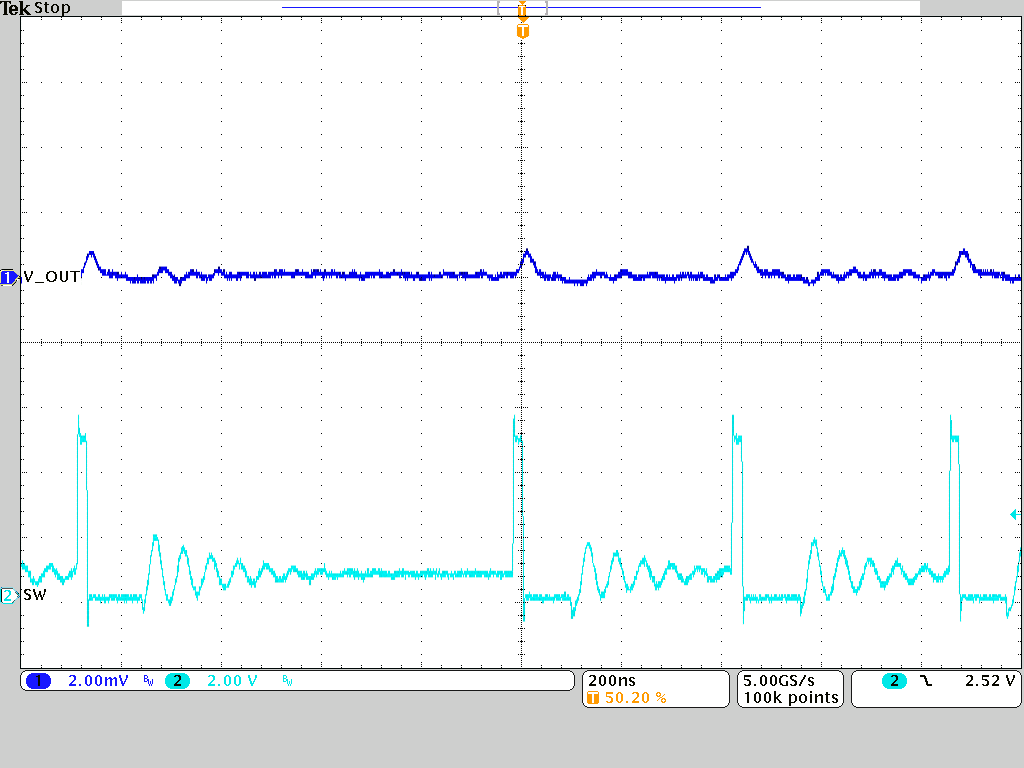
TPSM8287A06 TPSM8287A10 TPSM8287A12 TPSM8287A15 PFM-DCM Operation TPSM8287A12BBS
Vout = 0.9 VIOUT = 100 mA
Figure 9-29 PFM-DCM Operation TPSM8287A12BBS
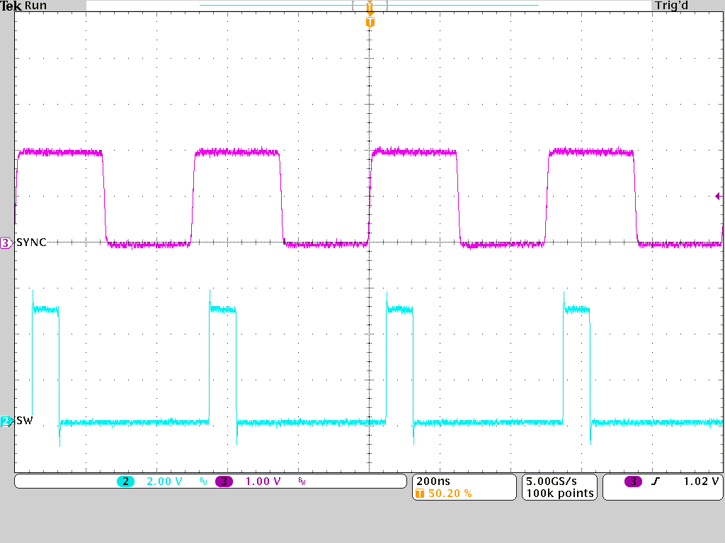
TPSM8287A06 TPSM8287A10 TPSM8287A12 TPSM8287A15 Synchronization to an External Clock

IOUT = 1 A

f(SYNC) = 2 MHz
Figure 9-31 Synchronization to an External Clock
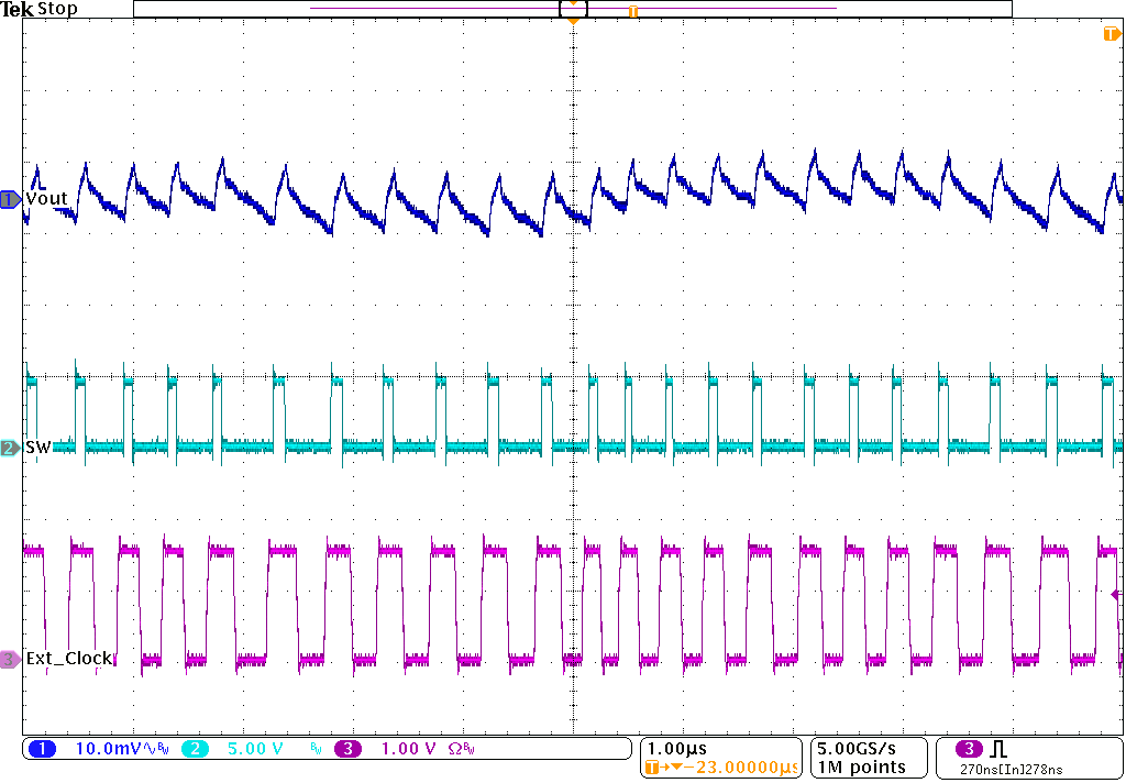
TPSM8287A06 TPSM8287A10 TPSM8287A12 TPSM8287A15 Synchronization to a Random External Clock

IOUT = 10 A

VOUT = 0.9 V

f(SYNC) = 2 to 2.5 MHz (random)

Figure 9-33 Synchronization to a Random External Clock
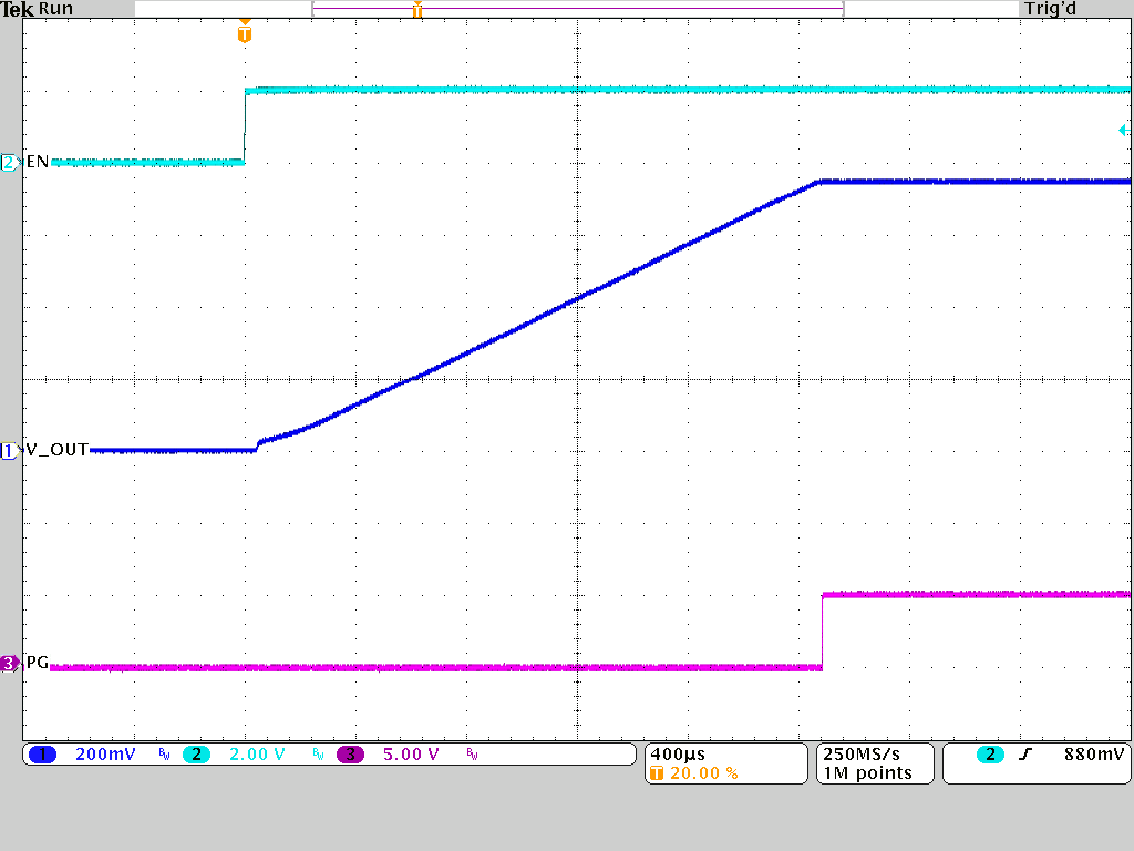
TPSM8287A06 TPSM8287A10 TPSM8287A12 TPSM8287A15 Start-Up Using EN Pin
VOUT = 0.75 V
Figure 9-35 Start-Up Using EN Pin
TPSM8287A06 TPSM8287A10 TPSM8287A12 TPSM8287A15 Shutdown Using EN Pin (Discharge Disabled)
VOUT = 3.3 VLoad = 7.5 Ω
Figure 9-37 Shutdown Using EN Pin (Discharge Disabled)
TPSM8287A06 TPSM8287A10 TPSM8287A12 TPSM8287A15 Safe Operating Area TPSM8287A06BAS VIN = 5.0 V

RΘJA = 19.5 °C/W

nat. convection

TJ,max = 125 °C

Figure 9-39 Safe Operating Area TPSM8287A06BAS VIN = 5.0 V
TPSM8287A06 TPSM8287A10 TPSM8287A12 TPSM8287A15 Safe Operating Area TPSM8287A10BAH VIN = 5.0 V

RΘJA = 20.0 °C/W

nat. convection

TJ,max = 125 °C

Figure 9-41 Safe Operating Area TPSM8287A10BAH VIN = 5.0 V
TPSM8287A06 TPSM8287A10 TPSM8287A12 TPSM8287A15 Safe Operating Area TPSM8287A12BAS VIN = 5.0 V

RΘJA = 19.5 °C/W

nat. convection

TJ,max = 125 °C

Figure 9-43 Safe Operating Area TPSM8287A12BAS VIN = 5.0 V
TPSM8287A06 TPSM8287A10 TPSM8287A12 TPSM8287A15 Safe Operating Area TPSM8287A12BBS VIN = 5.0 V
RΘJA = 19.5 °C/Wnat. convectionTJ,max = 125°C
Figure 9-45 Safe Operating Area TPSM8287A12BBS VIN = 5.0 V
TPSM8287A06 TPSM8287A10 TPSM8287A12 TPSM8287A15 Safe Operating Area TPSM8287A15BAH VIN = 5.0 V
RΘJA = 20.0 °C/Wnat. convectionTJ,max = 125°C
Figure 9-47 Safe Operating Area TPSM8287A15BAH VIN = 5.0 V
TPSM8287A06 TPSM8287A10 TPSM8287A12 TPSM8287A15 Safe Operating Area TPSM8287A15BBH VIN = 5.0 V
RΘJA = 20.0°C/Wnat. convectionTJ,max = 125°C
Figure 9-49 Safe Operating Area TPSM8287A15BBH VIN = 5.0 V