SLVSH48A May 2024 – September 2024 TPS7H1121-SP
PRODMIX
- 1
- 1 Features
- 2 Applications
- 3 Description
- 4 Device Options
- 5 Pin Configuration and Functions
- 6 Specifications
- 7 Parameter Measurement Information
-
8 Detailed Description
- 8.1 Overview
- 8.2 Functional Block Diagram
- 8.3 Feature Description
- 8.4 Device Functional Modes
-
9 Application and Implementation
- 9.1 Application Information
- 9.2
Typical Application
- 9.2.1 Design Requirements
- 9.2.2
Detailed Design Procedure
- 9.2.2.1 Output Voltage Configuration
- 9.2.2.2 Output Voltage Accuracy
- 9.2.2.3 Enable Threshold
- 9.2.2.4 Soft Start Capacitor
- 9.2.2.5 Programmable Current Limit Resistor
- 9.2.2.6 Characterization of Overcurrent Events that Exceed Thermal Limits
- 9.2.2.7 Power Good Pull Up Resistor
- 9.2.2.8 Capacitors
- 9.2.2.9 Frequency Compensation
- 9.3 Power Supply Recommendations
- 9.4 Layout
- 10Device and Documentation Support
- 11Revision History
- 12Mechanical, Packaging, and Orderable Information
7 Parameter Measurement Information

A. VOUT(SET) is the configured output voltage of the regulator
using the feedback resistors, VOUT(NOM) is the measured output
voltage. VIN is set 2V above the output (limited to 14V maximum) and
is decreased to the output voltage set point (VOUT(SET)). When
VOUT falls to 98% of the nominal value (VOUT(NOM)),
the dropout voltage is recorded.
Figure 7-1 Dropout
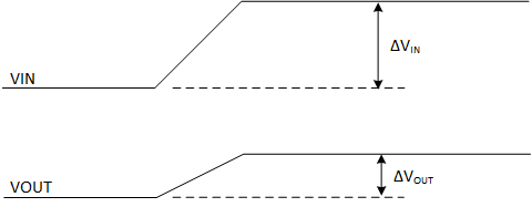
A. ΔVOUT / ΔVIN = 100µV/V (typ). This means for a 1V
change in VIN (ΔVIN = 1V), there will be a 100µV change in
VOUT (ΔVOUT = 100µV). Line regulation is a DC
parameter; therefore this waveform can only be considered valid after transients
die out or for a slow VIN slew rate.
Figure 7-2 Line Regulation
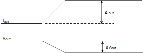
A. ΔVOUT / ΔIOUT = 4mV/A (typ). This means for a 1A
change in IOUT (ΔIOUT = 1A), there will be a 4mV change in
VOUT (ΔVOUT = 4mV). Load regulation is a DC parameter;
therefore this waveform can be considered valid after transients die out or for
a slow IOUT slew rate.
Figure 7-3 Load Regulation Figure 7-4 Enable Propagation Delay
 Figure 7-5 Soft Start Time