SLVSHI5 April 2024 TPS23881B
PRODUCTION DATA
- 1
- 1 Features
- 2 Applications
- 3 Description
- 4 Device Comparison Table
- 5 Pin Configuration and Functions
- 6 Specifications
- 7 Parameter Measurement Information
-
8 Detailed Description
- 8.1 Overview
- 8.2 Functional Block Diagram
- 8.3 Feature Description
- 8.4 Device Functional Modes
- 8.5 I2C Programming
- 8.6
Register Maps
- 8.6.1 Complete Register Set
- 8.6.2
Detailed Register Descriptions
- 8.6.2.1 INTERRUPT Register
- 8.6.2.2 INTERRUPT MASK Register
- 8.6.2.3 POWER EVENT Register
- 8.6.2.4 DETECTION EVENT Register
- 8.6.2.5 FAULT EVENT Register
- 8.6.2.6 START/ILIM EVENT Register
- 8.6.2.7 SUPPLY and FAULT EVENT Register
- 8.6.2.8 CHANNEL 1 DISCOVERY Register
- 8.6.2.9 CHANNEL 2 DISCOVERY Register
- 8.6.2.10 CHANNEL 3 DISCOVERY Register
- 8.6.2.11 CHANNEL 4 DISCOVERY Register
- 8.6.2.12 POWER STATUS Register
- 8.6.2.13 PIN STATUS Register
- 8.6.2.14 OPERATING MODE Register
- 8.6.2.15 DISCONNECT ENABLE Register
- 8.6.2.16 DETECT/CLASS ENABLE Register
- 8.6.2.17 Power Priority / 2Pair PCUT Disable Register Name
- 8.6.2.18 TIMING CONFIGURATION Register
- 8.6.2.19 GENERAL MASK Register
- 8.6.2.20 DETECT/CLASS RESTART Register
- 8.6.2.21 POWER ENABLE Register
- 8.6.2.22 RESET Register
- 8.6.2.23 ID Register
- 8.6.2.24 Connection Check and Auto Class Status Register
- 8.6.2.25 2-Pair Police Ch-1 Configuration Register
- 8.6.2.26 2-Pair Police Ch-2 Configuration Register
- 8.6.2.27 2-Pair Police Ch-3 Configuration Register
- 8.6.2.28 2-Pair Police Ch-4 Configuration Register
- 8.6.2.29 Capacitance (Legacy PD) Detection
- 8.6.2.30 Power-on Fault Register
- 8.6.2.31 PORT RE-MAPPING Register
- 8.6.2.32 Channels 1 and 2 Multi Bit Priority Register
- 8.6.2.33 Channels 3 and 4 Multi Bit Priority Register
- 8.6.2.34 4-Pair Wired and Port Power Allocation Register
- 8.6.2.35 4-Pair Police Ch-1 and 2 Configuration Register
- 8.6.2.36 4-Pair Police Ch-3 and 4 Configuration Register
- 8.6.2.37 TEMPERATURE Register
- 8.6.2.38 4-Pair Fault Configuration Register
- 8.6.2.39 INPUT VOLTAGE Register
- 8.6.2.40 CHANNEL 1 CURRENT Register
- 8.6.2.41 CHANNEL 2 CURRENT Register
- 8.6.2.42 CHANNEL 3 CURRENT Register
- 8.6.2.43 CHANNEL 4 CURRENT Register
- 8.6.2.44 CHANNEL 1 VOLTAGE Register
- 8.6.2.45 CHANNEL 2 VOLTAGE Register
- 8.6.2.46 CHANNEL 3 VOLTAGE Register
- 8.6.2.47 CHANNEL 4 VOLTAGE Register
- 8.6.2.48 2x FOLDBACK SELECTION Register
- 8.6.2.49 FIRMWARE REVISION Register
- 8.6.2.50 I2C WATCHDOG Register
- 8.6.2.51 DEVICE ID Register
- 8.6.2.52 CHANNEL 1 DETECT RESISTANCE Register
- 8.6.2.53 CHANNEL 2 DETECT RESISTANCE Register
- 8.6.2.54 CHANNEL 3 DETECT RESISTANCE Register
- 8.6.2.55 CHANNEL 4 DETECT RESISTANCE Register
- 8.6.2.56 CHANNEL 1 DETECT CAPACITANCE Register
- 8.6.2.57 CHANNEL 2 DETECT CAPACITANCE Register
- 8.6.2.58 CHANNEL 3 DETECT CAPACITANCE Register
- 8.6.2.59 CHANNEL 4 DETECT CAPACITANCE Register
- 8.6.2.60 CHANNEL 1 ASSIGNED CLASS Register
- 8.6.2.61 CHANNEL 2 ASSIGNED CLASS Register
- 8.6.2.62 CHANNEL 3 ASSIGNED CLASS Register
- 8.6.2.63 CHANNEL 4 ASSIGNED CLASS Register
- 8.6.2.64 AUTO CLASS CONTROL Register
- 8.6.2.65 CHANNEL 1 AUTO CLASS POWER Register
- 8.6.2.66 CHANNEL 2 AUTO CLASS POWER Register
- 8.6.2.67 CHANNEL 3 AUTO CLASS POWER Register
- 8.6.2.68 CHANNEL 4 AUTO CLASS POWER Register
- 8.6.2.69 ALTERNATIVE FOLDBACK Register
- 8.6.2.70 SRAM CONTROL Register
- 9 Application and Implementation
- 10Device and Documentation Support
- 11Revision History
- 12Mechanical, Packaging, and Orderable Information
9.4.1.1 Kelvin Current Sensing Resistors
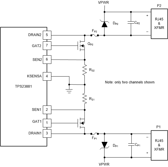
Load current in each PSE channel is sensed as the voltage across a low-end current-sense resistor with a value of 200 mΩ. For more accurate current sensing, kelvin sensing of the low end of the current-sense resistor is provided through pins KSENSA for channels 1 and 2, KSENSB for channels 3 and 4, KSENSC for channels 5 and 6 and KSENSD for channels 7 and 8.
 Figure 9-28 Kelvin Current-Sense Connection
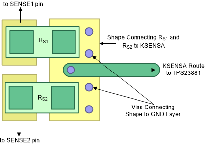
KSENSA is shared between SEN1 and SEN2, KSENSB is shared between SEN3 and SEN4, KSENSC is shared between SEN5 and SEN6, and KSENSD is shared between SEN7 and SEN8. To optimize the accuracy of the measurement, the PCB layout must be done carefully to minimize impact of PCB trace resistance. Refer to Figure 9-29 as an example.
 Figure 9-29 Kelvin
Sense Layout Example