SLVSHT1 August 2024 TPS55287-Q1
PRODUCTION DATA
- 1
- 1 Features
- 2 Applications
- 3 Description
- 4 Pin Configuration and Functions
- 5 Specifications
-
6 Detailed Description
- 6.1 Overview
- 6.2 Functional Block Diagram
- 6.3
Feature Description
- 6.3.1 VCC Power Supply
- 6.3.2 EXTVCC Power Supply
- 6.3.3 I2C Address Selection
- 6.3.4 Input Undervoltage Lockout
- 6.3.5 Enable and Programmable UVLO
- 6.3.6 Soft Start
- 6.3.7 Shutdown and Load Discharge
- 6.3.8 Switching Frequency
- 6.3.9 Switching Frequency Dithering
- 6.3.10 Inductor Current Limit
- 6.3.11 Internal Charge Path
- 6.3.12 Output Voltage Setting
- 6.3.13 Output Current Monitoring and Cable Voltage Droop Compensation
- 6.3.14 Output Current Limit
- 6.3.15 Overvoltage Protection
- 6.3.16 Output Short Circuit Protection
- 6.3.17 Thermal Shutdown
- 6.4 Device Functional Modes
- 6.5 Programming
-
7 Register Maps
- 7.1 REF Register (Address = 0h, 1h) [reset = 10100100b, 00000001b]
- 7.2 IOUT_LIMIT Register (Address = 2h) [reset = 11100100b]
- 7.3 VOUT_SR Register (Address = 3h) [reset = 00000001b]
- 7.4 VOUT_FS Register (Address = 4h) [reset = 00000011b]
- 7.5 CDC Register (Address = 5h) [reset = 11100000b]
- 7.6 MODE Register (Address = 6h) [reset = 00100000b]
- 7.7 STATUS Register (Address = 7h) [reset = 00000011b]
- 7.8 Register Summary
- 8 Application and Implementation
- 9 Device and Documentation Support
- 10Revision History
- 11Mechanical, Packaging, and Orderable Information
6.3.13 Output Current Monitoring and Cable Voltage Droop Compensation
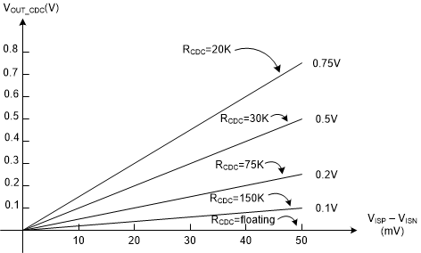
The TPS55287-Q1 outputs a voltage at the CDC pin proportional to the sensed voltage across an output current sensing resistor between the ISP pin and the ISN pin. Equation 6 shows the exact voltage at the CDC pin related to the sensed output current.

To compensate the voltage droop across a cable from the output of the USB port to its powered device, the TPS55287-Q1 can lift its output voltage in proportion to the load current. There are two methods in the TPS55287-Q1 to implement the compensation: by setting internal register 05h or by placing a resistor between the CDC pin and AGND pin.
When using internal output voltage feedback, it is recommended to use the internal compensation setting. When using an external resistor divider at the FB/INT pin to set the output voltage, it is recommended to use the external compensation setting by placing a resistor at the CDC pin.
By default, the internal cable voltage droop compensation function is enabled with 0V added to the output voltage. Write the value into the bit CDC [2:0] in register 05h to get the desired voltage compensation.
When using external output voltage feedback, external compensation is better than the internal register for its high accuracy. The output voltage rises in proportion to the current sourcing from the CDC pin through the resistor at the CDC pin. It is recommended to use 100kΩ resistance for the up resistor of the feedback resistor divider. Equation 7 shows the output voltage rise related to the sensed output current, the resistance at the CDC pin, and the up resistor of the output voltage feedback resistor divider.

where
- RFB_UP is the up resistor of the resistor divider between the output and the FB/INT pin
- RCDC is the resistor at the CDC pin
When RFB_UP is 100kΩ, the output voltage rise versus the sensed output current and the resistor at the CDC pin is shown in Figure 6-6.
 Figure 6-6 Output Voltage Rise versus Output Current