SLVU300A June 2009 – October 2021 TPS54325
3.1 Layout
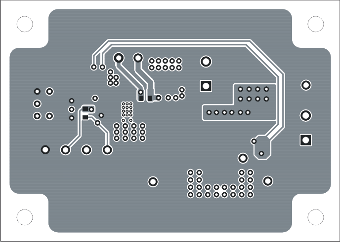
The board layout for the TPS54325EVM and is shown in Figure 3-1 through Figure 3-6. The top layer contains the main power traces for VIN , VOUT and the SW1 and SW2 nodes. Also on the top layer are connections for the pins of the TPS54325 and a large area filled with power ground (PGND) connected to pins 8 and 9 of the TPS54325. The first internal layer is a split ground plane containing a large power ground (PGND) area and a smaller signal ground (GND) area. The second internal layer contains an additional VIN trace and a connection from switch SW1 to VCC. The remainder of the second internal layer is power ground (PGND) area. The bottom layer contans the remainder of the circuit interconnect traces and the signal ground plane (GND) that is connected to pin 5 of the TPS54325 through a via near the pin. The signal ground and power ground are electrically common. They are connected together on the pcb at the pin 5 and the powerpad of the TPS54325. The bottom assembly layer is shown as looking from the back side of the printed circuit board.
The input decoupling capacitor and all parts are located as close to the IC as possible.
 Figure 3-1 Top Assembly
 Figure 3-2 Top Layer
 Figure 3-3 Internal Layer 1
 Figure 3-4 Internal Layer 2
 Figure 3-5 Bottom Layer
 Figure 3-6 Bottom Assembly (as Viewed from Back Side)