SLVU433A February 2011 – January 2022 TPS53125 , TPS53126 , TPS53127 , TPS53128 , TPS53129
- Trademarks
- 1 Introduction
- 2 Electrical Performance Specifications
- 3 Schematics
-
4 Connector and Test Point Descriptions
- 4.1 Enable Switches (SW1 and SW2)
- 4.2 Switching Frequency Select Switch (SW3)
- 4.3
Test Point Descriptions
- 4.3.1 Input Voltage Monitoring (TP3 and TP9)
- 4.3.2 Channel 1 Output Voltage Monitoring (TP4 and TP8)
- 4.3.3 Channel 2 Output Voltage Monitoring (TP6 and TP7)
- 4.3.4 Soft-Start Voltage Monitoring (TP1, TP2, and TP3)
- 4.3.5 Switching Node Monitoring (TP3, TP5, and TP11)
- 4.3.6 5-V Regulator Output Monitoring (TP3 and TP10)
- 5 Test Setup
- 6 Test Procedure
- 7 Performance Data and Typical Characteristic Curves
- 8 EVM Assembly Drawings and Layout
- 9 Bill of Materials
- 10Revision History
8 EVM Assembly Drawings and Layout
Figure 8-1 through Figure 8-6 show the design of the TPS53128EVM-620 printed circuit board. The EVM has been designed using a 4-layer, 2-oz copper-clad circuit board of 3.5 inch by 2.7 inch to allow the user to easily view, probe, and evaluate the TPS53128 control IC in a practical application. Moving components to both sides of the PCB or using additional internal layers can offer additional size reduction for space constrained systems.
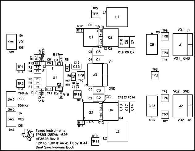 Figure 8-1 Top Assembly
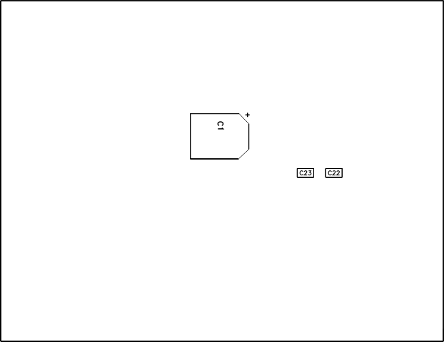 Figure 8-2 Bottom Assembly
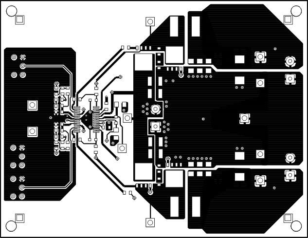 Figure 8-3 Top Layer
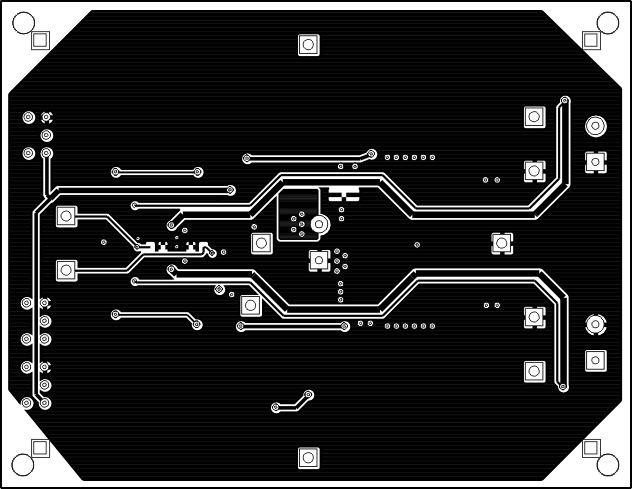 Figure 8-4 Bottom Layer
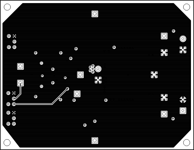 Figure 8-5 Internal Layer 1
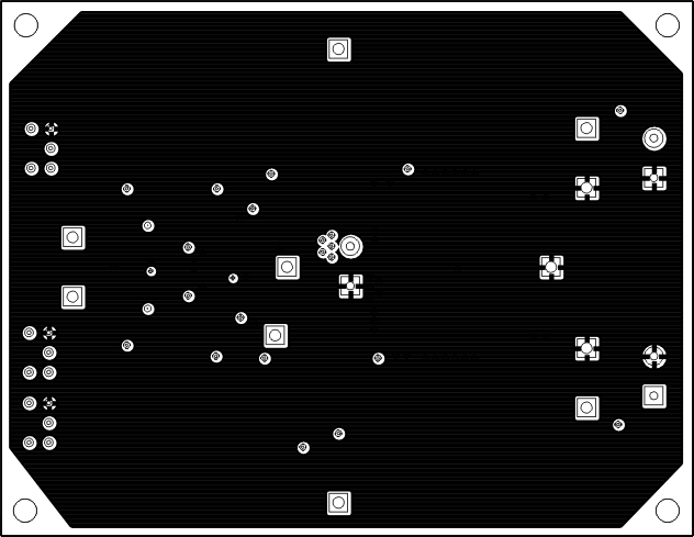 Figure 8-6 Internal Layer 2