SLVU445C March   2011  – August 2021 TPS56121


  1.   Trademarks
  2. Introduction
  3. Description
    1. 2.1 Applications
    2. 2.2 Features
  4. Electrical Performance Specifications
  5. Schematic
  6. Test Setup
    1. 5.1 Test Equipment
      1. 5.1.1 Voltage Source
      2. 5.1.2 Meters
      3. 5.1.3 Load
      4. 5.1.4 Oscilloscope
      5. 5.1.5 Fan
    2. 5.2 Recommended Wire Gauge
      1. 5.2.1 VIN to J1
      2. 5.2.2 J2 to LOAD
    3. 5.3 Equipment Set Up Procedure
  7. Configurations
    1. 6.1 Enable Selection (J3)
  8. Test Point Descriptions
    1. 7.1 Input Voltage Monitoring (TP1 and TP2)
    2. 7.2 Output Voltage Monitoring (TP3 and TP4)
    3. 7.3 Enable/Soft-start Monitoring (TP5)
    4. 7.4 Power Good Monitoring (TP6)
    5. 7.5 Loop Response Testing (TP7, TP8, TP9 and TP10)
    6. 7.6 Switch Node Voltage Monitoring (TP11 and TP12)
  9. Test Procedures
    1. 8.1 Start Up/Shut Down Procedure
    2. 8.2 Output Ripple Voltage Measurement Procedure
    3. 8.3 Control Loop Gain and Phase Measurement Procedure
    4. 8.4 Equipment Shutdown
  10. Performance Data and Typical Characteristic Curves
    1. 9.1  Efficiency
    2. 9.2  Load Regulation
    3. 9.3  Line Regulation
    4. 9.4  Output Voltage Ripple
    5. 9.5  Switch Node
    6. 9.6  Load Transient
    7. 9.7  Start Up
    8. 9.8  Power Off
    9. 9.9  Over-Current Protection
    10. 9.10 Control Loop Bode Plot
    11. 9.11 Thermal Image
  11. 10EVM Assembly Drawings and PCB Layout
  12. 11List of Materials
  13. 12Revision History

EVM Assembly Drawings and PCB Layout

The following figures (Figure 10-1 through Figure 10-6) show the design of the TPS56121EVM-601 printed circuit board. The EVM has been designed using a 4-layer, 2-oz copper-clad circuit board 2.5” x 2.5” with components on both sides of the PCB to allow the user to view, probe and evaluate the TPS56121 high current converter with integrated FETs in a small form factor, high-current application.
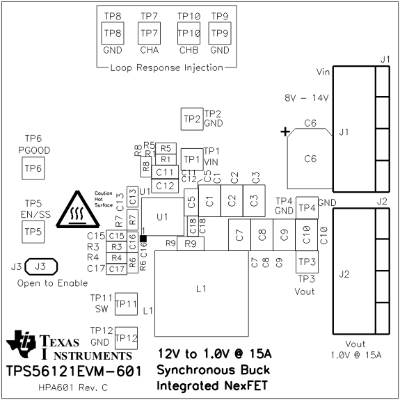
GUID-CAD6470A-9955-42E6-BC22-716AB32403D6-low.gifFigure 10-1 TPS56121EVM-601 Top Assembly Drawing (top view)
GUID-279A567C-8EC6-4F2D-85CC-2AC42DD4BE70-low.gifFigure 10-2 TPS56121EVM-601 Bottom Assembly Drawing (bottom view)
GUID-30287C2D-CAB7-41A1-A7C1-F7834DB7196B-low.gifFigure 10-3 TPS56121EVM-601 Top Copper (top view)
GUID-335BCA88-9C6D-425F-8F4F-20FACE9BF001-low.gifFigure 10-4 TPS56121EVM-601 Internal 1 (top view)
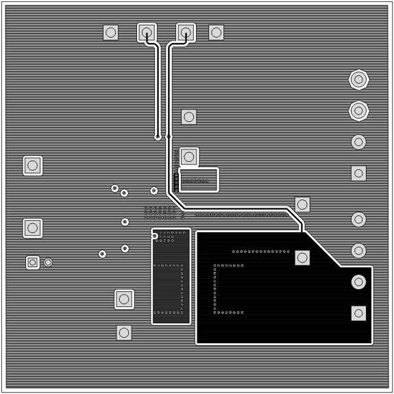
GUID-BF1C58F3-A620-4B3B-BDCF-C85518181243-low.gifFigure 10-5 TPS56121EVM-601 Internal 2 (top view)
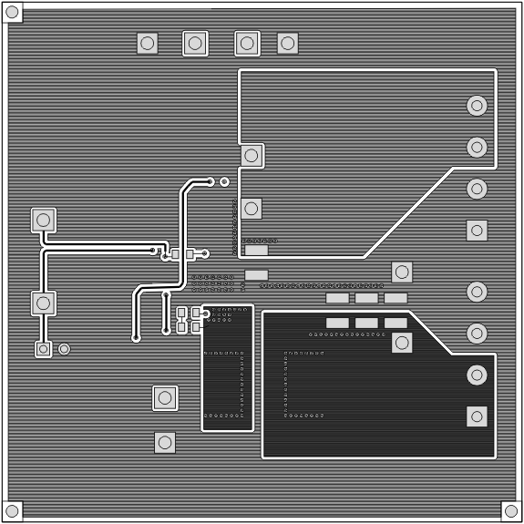
GUID-DC7B9363-E7C3-4B28-8C69-3F8457A4C1CD-low.gifFigure 10-6 TPS56121EVM-601 Bottom Copper (top view)