SLVU469B June 2011 – May 2021 TPS65253
3 Schematic
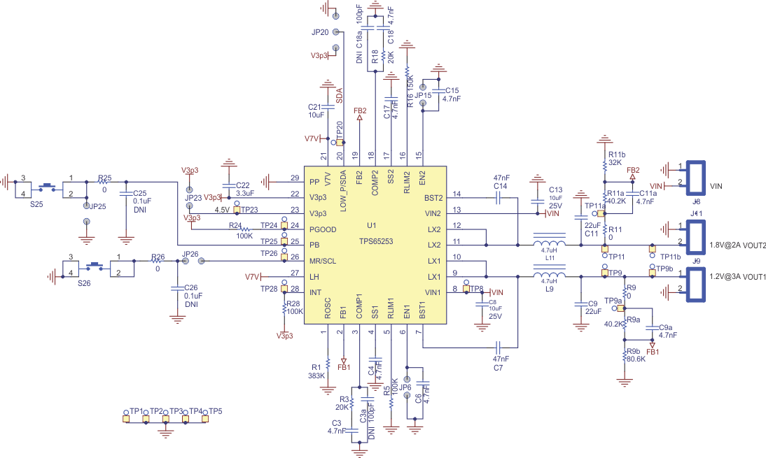
Figure 3-1 illustrates the TPS65253 EVM schematic.
The resistor and capacitor values have been chosen according to the guidelines presented on the TPS65253 spec available at http://focus.ti.com/docs/prod/folders/print/TPS65253.html.
Note that for the purpose of gains-phase measurements R9 and R11 (0 Ω on the EVM) need to be replaced by suitable low value resistors as per the network analyzer setup required. Test points are provided on either end of the resistors to allow for easy measurement. Also, R3, R4, C10, and C12 can be populated if users desire to reduce overshoot at LX pins due to parasitic L and C resonance.
 Figure 3-1 TPS65253 Schematic