SLVU488A October 2011 – October 2021 TPS54329
6.1 Schematic
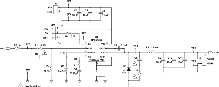
Figure 6-1 is the schematic for the TPS54329EVM-056.
 Figure 6-1 TPS54329EVM-056 Schematic Diagram
SLVU488A October 2011 – October 2021 TPS54329
Figure 6-1 is the schematic for the TPS54329EVM-056.
 Figure 6-1 TPS54329EVM-056 Schematic Diagram