SLVU793A October 2012 – June 2021 TPS56921
2.6 Loop Characteristics
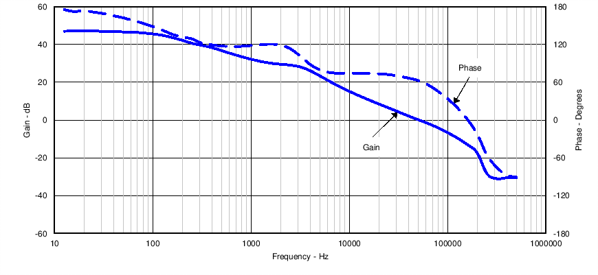
Figure 2-6 shows the TPS56921EVM-188 loop-response characteristics when the output voltage is set by the external resistor divider network. Gain and phase plots are shown for VIN voltage of 12 V. Load current for the measurement is 4 A.
 Figure 2-6 TPS56921EVM-188 Loop Response, VOUT Set by Resistor Divider
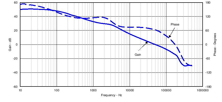
Figure 2-7 shows the TPS56921EVM-188 loop-response characteristics when the output voltage is set by the external resistor divider network. Gain and phase plots are shown for VIN voltage of 12 V. Load current for the measurement is 4 A.
 Figure 2-7 TPS56921EVM-188 Loop Response, VOUT Set by I2C Interface