SLVU888A April 2013 – August 2021 TPS54628
5.1 Layout
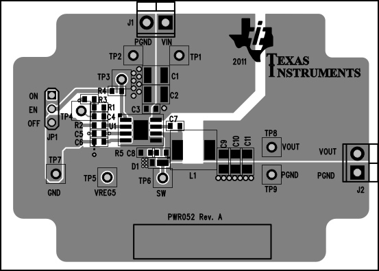
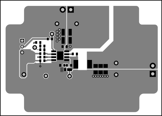
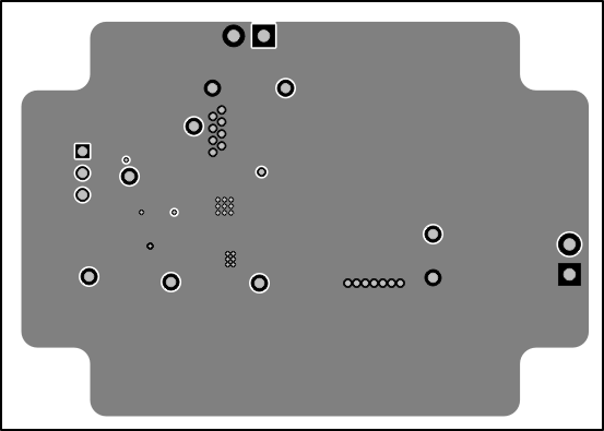
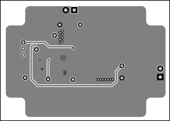
The board layout for the TPS54628EVM-052 is shown in Figure 5-1 through Figure 5-5. The top layer contains the main power traces for VIN, VOUT, and ground. Also on the top layer are connections for the pins of the TPS54628 and a large area filled with ground. Most of the signal traces also are located on the top side. The input decoupling capacitors are located as close to the IC as possible. The input and output connectors, test points, and all of the components are located on the top side. An analog ground (GND) area is provided on the top side. Analog ground (GND) and power ground (PGND) are connected at a single point on the top layer near C6. The two internal layers are completely dedicated to power ground planes. The bottom layer is primarily power ground. Traces also connect VIN to the enable control jumper, VREG5 test points and the feedback trace from VOUT to the voltage setpoint divider network.
 Figure 5-1 Top Assembly
 Figure 5-2 Top Layer
 Figure 5-3 Internal Layer 1
 Figure 5-4 Internal Layer 2
 Figure 5-5 Bottom Layer