SLVU988A October   2013  – June 2021 TPS56628


  1.   Trademarks
  2. 1Introduction
  3. 2Performance Specification Summary
  4. 3Modifications
    1. 3.1 Output Voltage Setpoint
    2. 3.2 Output Filter and Closed-Loop Response
  5. 4Test Setup and Results
    1. 4.1  Input and Output Connections
    2. 4.2  Start-Up Procedure
    3. 4.3  Efficiency
    4. 4.4  Load Regulation
    5. 4.5  Line Regulation
    6. 4.6  Load Transient Response
    7. 4.7  Output Voltage Ripple
    8. 4.8  Input Voltage Ripple
    9. 4.9  Start-Up
    10. 4.10 Shut-Down
  6. 5Board Layout
    1. 5.1 Layout
  7. 6Schematic, Bill of Materials, and Reference
    1. 6.1 Schematic
    2. 6.2 Bill of Materials
    3. 6.3 Reference
  8. 7Revision History

Shut-Down

The TPS56628EVM-534 shut-down waveforms relative to VIN and EN are shown in Figure 4-12 and Figure 4-13. RLOAD = 2 Ω.
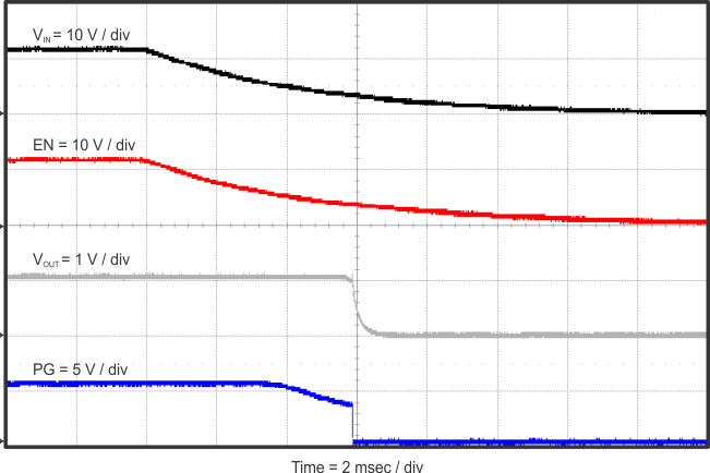
GUID-E7D7611D-F953-4D63-93A4-4463BDA93B75-low.gif Figure 4-12 TPS56628EVM-534 Shut-Down Relative to VIN With VREG5, PG and VOUT
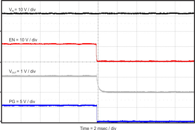
GUID-E2DF1B89-BAB3-4CD5-9B81-321F87335CF2-low.gif Figure 4-13 TPS56628EVM-534 Shut-Down Relative to EN With VREG5, PG and VOUT