SLVUA85A June 2014 – May 2021 TPS65261
3 Board Layout
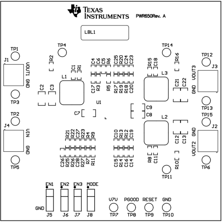
Figure 3-1 illustrates the PCB layout for this EVM.
 Figure 3-1 Component Placement (Top Layer)
SLVUA85A June 2014 – May 2021 TPS65261
Figure 3-1 illustrates the PCB layout for this EVM.
 Figure 3-1 Component Placement (Top Layer)