SLVUAD3A March   2015  – May 2021 TPS62184


  1.   Trademarks
  2. 1Introduction
    1. 1.1 Performance Specification
    2. 1.2 Modifications
      1. 1.2.1 Changing the Output Voltage
      2. 1.2.2 Input and Output Capacitors
      3. 1.2.3 Lower Profile Solutions
      4. 1.2.4 Configurable Enable Threshold Voltage
  3. 2Setup
    1. 2.1 Input/Output Connector Descriptions
    2. 2.2 Setup
  4. 3TPS62184EVM-581 Test Results
  5. 4Board Layout
  6. 5Schematic and Bill of Materials
    1. 5.1 Schematic
    2. 5.2 Bill of Materials
  7. 6Revision History

Board Layout

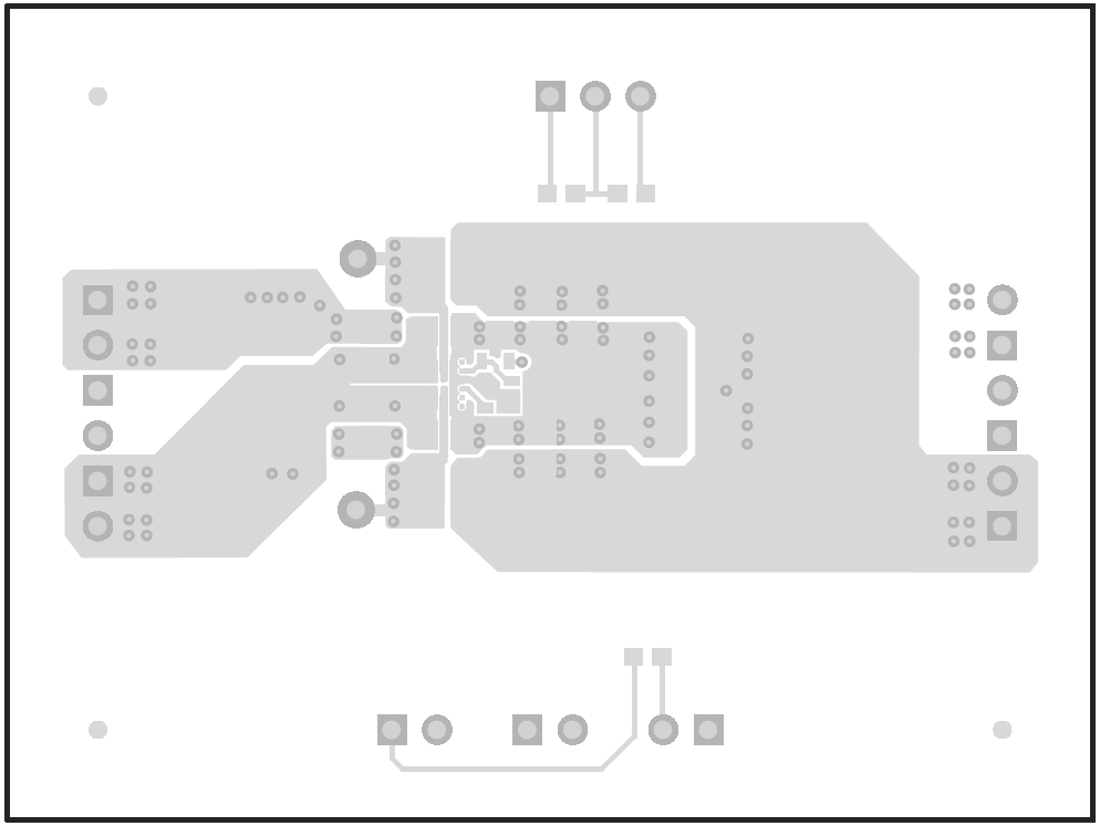
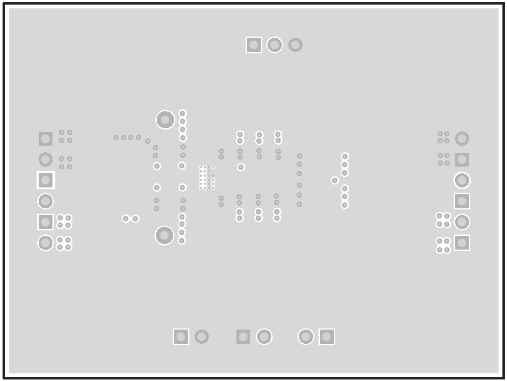
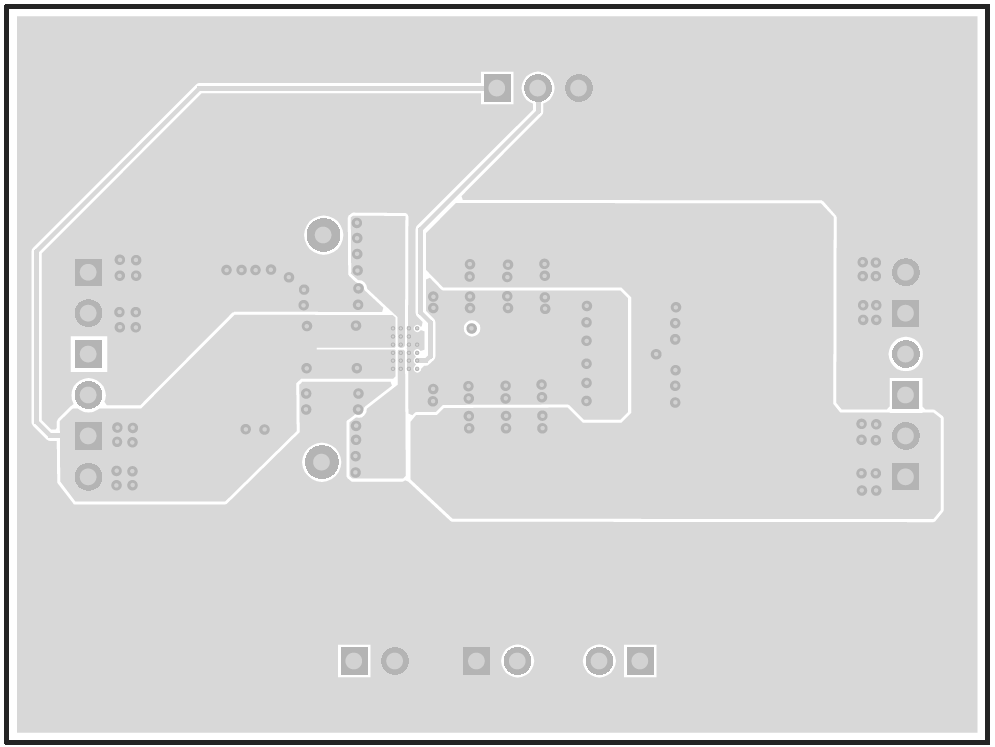
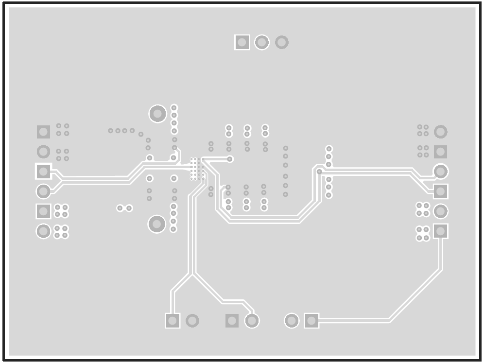
This section provides the TPS62184EVM-581 board layout and illustrations. The Gerbers are available on the EVM product page: TPS62184EVM-581. Rev. B of the PCB just filled the vias under U1 to improve manufacturability. No copper changes were made from Rev. A.
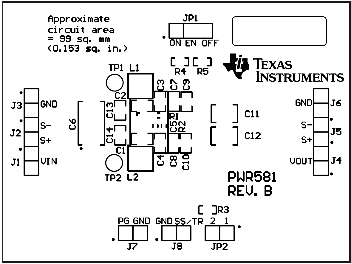
GUID-CF9528C8-EFC1-4E71-9EE7-54988005FCC8-low.png Figure 4-1 Assembly Layer
GUID-2D1FD997-07B8-41E5-A4E0-BD94EBCD1D1B-low.png Figure 4-2 Top Silk Layer
GUID-71C314B5-AF22-4A64-A8C0-CC0CF67C0750-low.png Figure 4-3 Top Layer
GUID-F7871244-0FA0-4C05-9B62-90449C95FBDB-low.png Figure 4-4 Internal Layer 1
GUID-444FE254-9035-4181-994F-B684698F9FC6-low.png Figure 4-5 Internal Layer 2
GUID-6DC90198-1BC7-4D0D-A049-2C38B1E8BA11-low.png Figure 4-6 Bottom Layer