TPS562219A Step-Down Converter Evaluation Module User's Guide
Trademarks
D-CAP2™ is a trademark of Texas Instruments.
All trademarks are the property of their respective owners.
1 Introduction
The TPS562219A is a single, adaptive on-time, D-CAP2™ mode, synchronous buck converter requiring a very low external component count. The D-CAP2 control circuit is optimized for low-ESR output capacitors such as POSCAP, SP-CAP, or ceramic types and features fast transient response with no external compensation. The slow start time is externally programmable and there is a dedicated Power Good (PG) pin to aid in voltage monitoring and sequencing. The switching frequency is internally set at a nominal 650 kHz. The high-side and low-side switching MOSFETs are incorporated inside the TPS562219A package along with the gate-drive circuitry. The low drain-to-source on resistance of the MOSFETs allows the TPS562219A to achieve high efficiencies and helps keep the junction temperature low at high output currents. The TPS562219A dc/dc synchronous converter is designed to provide up to a 2-A output from an input voltage source of 4.5 V to 17 V. The output voltage range is from 0.8 V to 6.5 V. Rated input voltage and output current ranges for the evaluation module are given in Table 1-1.
The TPS562219AEVM-663 evaluation module (EVM) is a single, synchronous buck converter providing 1.05 V at 2 A from 4.5-V to 17-V input. This user’s guide describes the TPS562219AEVM-663 performance.
| EVM | Input Voltage Range | Output Current Range |
|---|---|---|
| TPS562219AEVM-663 | VIN = 4.5 V to 17 V | 0 A to 2 A |
2 Performance Specification Summary
A summary of the TPS562219AEVM-663 performance specifications is provided in Table 2-1. Specifications are given for an input voltage of VIN = 12 V and an output voltage of 1.05 V, unless otherwise noted. The ambient temperature is 25°C for all measurement, unless otherwise noted.
| Specifications | Test Conditions | Min | Typ | Max | Unit | |
|---|---|---|---|---|---|---|
| Input voltage range (VIN) | 4.5 | 12 | 17 | V | ||
| CH1 | Output voltage | 1.05 | V | |||
| Operating frequency | VIN = 12 V, IO = 2 A | 650 | kHz | |||
| Output current range | 0 | 2 | A | |||
| Over current limit | VIN = 12 V, LO = 1.5 µH | A | ||||
| Output ripple voltage | VIN = 12 V, IO = 2 A | 20 | mVPP | |||
3 Modifications
These evaluation modules are designed to provide access to the features of the TPS562219A. Some modifications can be made to this module.
3.1 Output Voltage Setpoint
To change the output voltage of the EVMs, it is necessary to change the value of resistor R1. Changing the value of R1 can change the output voltage above 0.765 V. The value of R1 for a specific output voltage can be calculated using Equation 1.
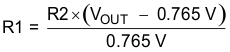
Table 3-1 lists the R1 values for some common output voltages. Note that the values given in Table 3-1 are standard values and not the exact value calculated using Table 3-1.
| Output Voltage (V) | R1 (kΩ) | R2 (kΩ) | L1 (µH) | C5 + C6 +C7 (µF) | ||
|---|---|---|---|---|---|---|
| Min | Typ | Max | ||||
| 1.0 | 3.09 | 10.0 | 1.5 | 2.2 | 4.7 | 20 - 68 |
| 1.05 | 3.74 | 10.0 | 1.5 | 2.2 | 4.7 | 20 - 68 |
| 1.2 | 5.76 | 10.0 | 1.5 | 2.2 | 4.7 | 20 - 68 |
| 1.5 | 9.53 | 10.0 | 1.5 | 2.2 | 4.7 | 20 - 68 |
| 1.8 | 13.7 | 10.0 | 1.5 | 2.2 | 4.7 | 20 - 68 |
| 2.5 | 22.6 | 10.0 | 2.2 | 3.3 | 4.7 | 20 - 68 |
| 3.3 | 33.2 | 10.0 | 2.2 | 3.3 | 4.7 | 20 - 68 |
| 5.0 | 54.9 | 10.0 | 3.3 | 4.7 | 4.7 | 20 - 68 |
| 6.5 | 75.0 | 10.0 | 3.3 | 4.7 | 4.7 | 20 - 68 |
