SLVUB76A July   2017  – October 2021 TPS54335A


  1.   Trademarks
  2. 1Introduction
    1. 1.1 Background
    2. 1.2 Performance Specification Summary
    3. 1.3 Modifications
      1. 1.3.1 Output Voltage Set Point
      2. 1.3.2 Adjustable UVLO
  3. 2Test Setup and Results
    1. 2.1  Input/Output Connections
    2. 2.2  Efficiency
    3. 2.3  Output Voltage Load Regulation
    4. 2.4  Output Voltage Line Regulation
    5. 2.5  Load Transients
    6. 2.6  Loop Characteristics
    7. 2.7  Output Voltage Ripple
    8. 2.8  Input Voltage Ripple
    9. 2.9  Powering Up
    10. 2.10 Powering Down
  4. 3Board Layout
    1. 3.1 Layout
  5. 4Schematic and Bill of Materials
    1. 4.1 Schematic
    2. 4.2 Bill of Materials
  6. 5Revision History

Powering Down

Figure 2-13 and Figure 2-14 show the start-up waveforms for the TPS54335AEVM-010. In Figure 2-13, the output voltage ramps down as soon as the input voltage falls below the UVLO stop threshold as set by the R1 and R2 resistor divider network. In Figure 2-14, the output is inhibited by using a jumper at JP1 to tie EN to GND. The input voltage for these plots is 24 V and the load is 5 Ω.

GUID-B7B04012-F73E-4AF0-AA79-29713050F403-low.gifFigure 2-13 TPS54335AEVM-010 Shut-down Relative to VIN
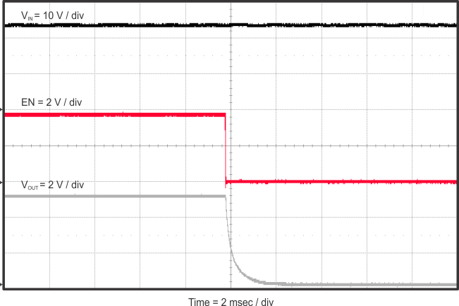
GUID-2609EDBF-2546-43FC-B953-E2C6300DF060-low.gifFigure 2-14 TPS54335AEVM-010 Shut-down Relative to EN