SLVUBB4B November 2017 – February 2023
- Abstract
- Trademarks
- 1 Topologies Window
- 2 FET Losses Calculator
- 3 Load Step Calculator
- 4 Capacitor Current Sharing Calculator
- 5 AC/DC Bulk Capacitor Calculator
- 6 RCD-Snubber Calculator for Flyback Converters
- 7 RC-Snubber Calculator
- 8 Output Voltage Resistor Divider
- 9 Dynamic Analog Output Voltage Scaling
- 10Dynamic Digital Output Voltage Scaling
- 11Unit Converter
-
12Loop Calculator
- 12.1 Inputs
- 12.2
Transfer Functions
- 12.2.1 Output Impedance Transfer Function
- 12.2.2 Transfer Function VMC Buck Power Stage
- 12.2.3 Transfer Function CMC Buck Power Stage
- 12.2.4 Transfer Function CMC Boost Power Stage
- 12.2.5 Transfer Function CMC Inverting Buck-Boost Power Stage
- 12.2.6 Transfer Function CMC Forward Power Stage
- 12.2.7 Transfer Function CMC Flyback Power Stage
- 12.2.8 Transfer Function Closed Loop
- 12.2.9 Transfer Function Isolated Type II Compensation Network With a Zener Clamp
- 12.2.10 Transfer Function Isolated Type II Compensation Network Without a Zener Clamp
- 13Filter Designer
- 14Additional Information
- 15Revision History
7 RC-Snubber Calculator
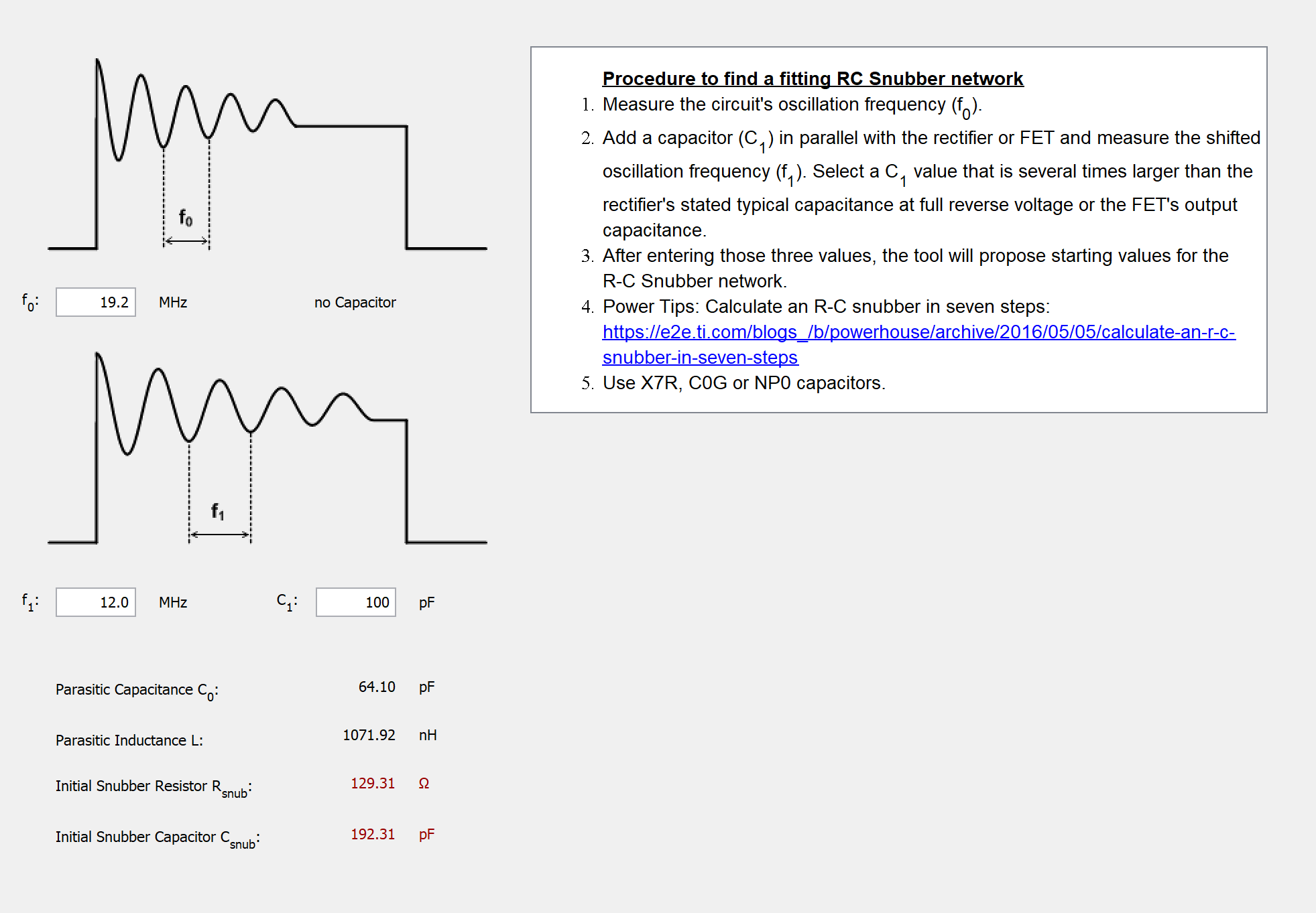
An RC-Snubber circuit is one option to reduce ringing in a switch mode power supply. Alternatives are the use of MOSFET gate resistors or a resistor in series with the bootstrap capacitor to slow down rise and/or fall times. With the RC-Snubber Calculator, Power Stage Designer helps the designer determine starting values for the snubber resistor and capacitor.
#T5147377-13 shows the RC-Snubber Calculator window.
 Figure 7-1 RC-Snubber Calculator Window
- Measure the oscillation frequency f0 of the circuit without a snubber network.
- Add a capacitor C1 in parallel with the rectifier or FET and measure the shifted oscillation frequency f1. Select a C1 value that is several times larger than the stated typical capacitance of the rectifier at full reverse voltage or the output capacitance of the FET.
- After entering these three values, the tool will propose starting values for the R-C Snubber network.
Frequency shift ratio:
Equation 17.
Parasitic capacitance:
Equation 18.
Parasitic inductance:
Equation 19.
Initial Snubber capacitance:
Equation 20.
Initial Snubber resistance:
Equation 21.