SLVUBB4B November 2017 – February 2023
- Abstract
- Trademarks
- 1 Topologies Window
- 2 FET Losses Calculator
- 3 Load Step Calculator
- 4 Capacitor Current Sharing Calculator
- 5 AC/DC Bulk Capacitor Calculator
- 6 RCD-Snubber Calculator for Flyback Converters
- 7 RC-Snubber Calculator
- 8 Output Voltage Resistor Divider
- 9 Dynamic Analog Output Voltage Scaling
- 10Dynamic Digital Output Voltage Scaling
- 11Unit Converter
-
12Loop Calculator
- 12.1 Inputs
- 12.2
Transfer Functions
- 12.2.1 Output Impedance Transfer Function
- 12.2.2 Transfer Function VMC Buck Power Stage
- 12.2.3 Transfer Function CMC Buck Power Stage
- 12.2.4 Transfer Function CMC Boost Power Stage
- 12.2.5 Transfer Function CMC Inverting Buck-Boost Power Stage
- 12.2.6 Transfer Function CMC Forward Power Stage
- 12.2.7 Transfer Function CMC Flyback Power Stage
- 12.2.8 Transfer Function Closed Loop
- 12.2.9 Transfer Function Isolated Type II Compensation Network With a Zener Clamp
- 12.2.10 Transfer Function Isolated Type II Compensation Network Without a Zener Clamp
- 13Filter Designer
- 14Additional Information
- 15Revision History
9 Dynamic Analog Output Voltage Scaling
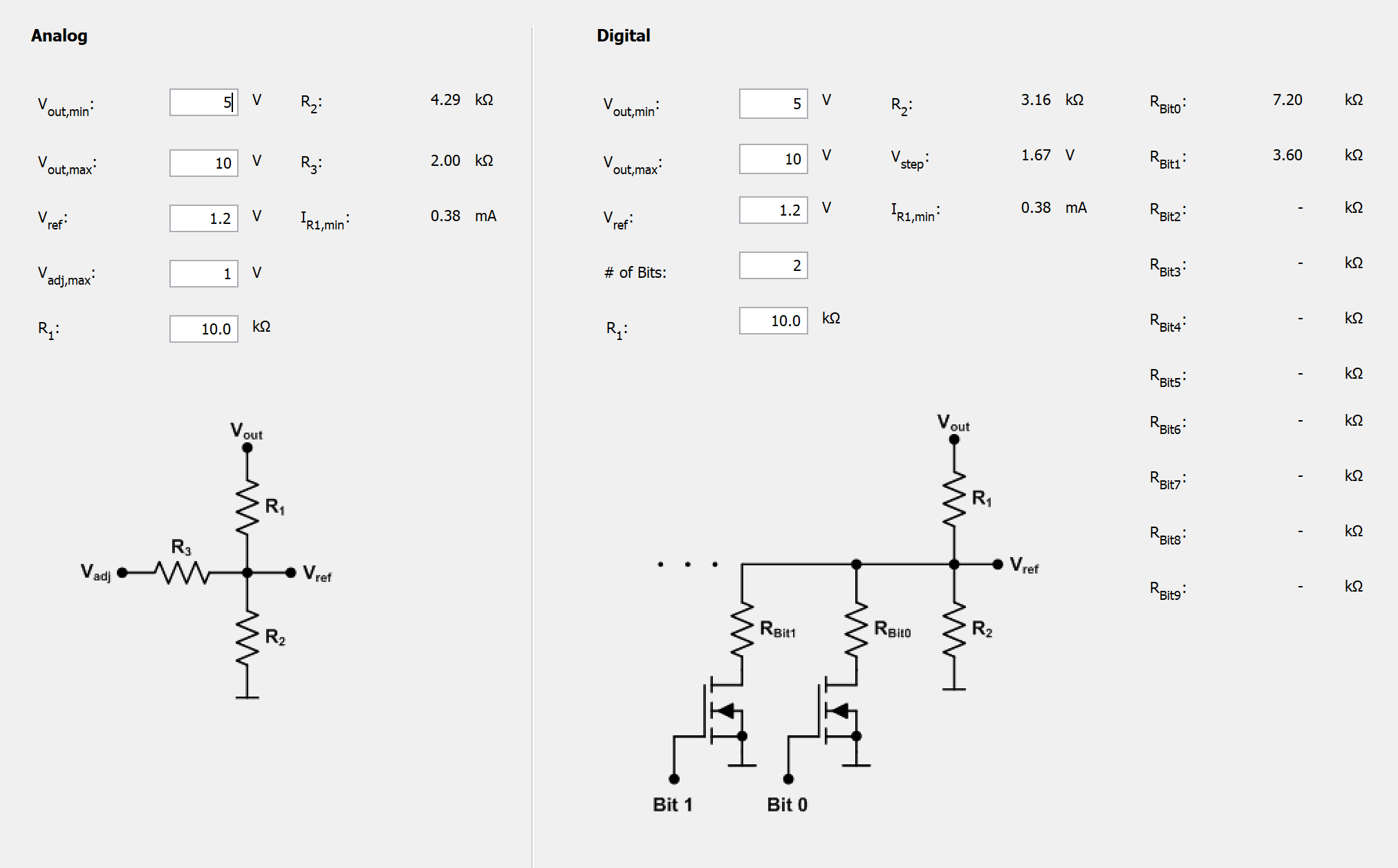
If the output voltage of a power supply must be adjustable, add a third resistor to the feedback resistor divider and apply an analog voltage to this resistor (for example, with the DAC of a microcontroller). The analog signal can also be provided by smoothing a PWM signal with a low-pass filter. After entering the minimum output voltage, maximum output voltage, reference voltage, maximum adjusting voltage signal, and the desired value for the top feedback resistor, Power Stage Designer calculates the required bottom feedback resistance and the adjusting voltage signal series resistance, as well as the minimum bias current going through the top feedback resistor.
#T5147377-30 shows the Dynamic Output Voltage Scaling Calculator window.
 Figure 9-1 Dynamic Output Voltage Scaling Calculator
Window