SLVUBB4B November 2017 – February 2023
- Abstract
- Trademarks
- 1 Topologies Window
- 2 FET Losses Calculator
- 3 Load Step Calculator
- 4 Capacitor Current Sharing Calculator
- 5 AC/DC Bulk Capacitor Calculator
- 6 RCD-Snubber Calculator for Flyback Converters
- 7 RC-Snubber Calculator
- 8 Output Voltage Resistor Divider
- 9 Dynamic Analog Output Voltage Scaling
- 10Dynamic Digital Output Voltage Scaling
- 11Unit Converter
-
12Loop Calculator
- 12.1 Inputs
- 12.2
Transfer Functions
- 12.2.1 Output Impedance Transfer Function
- 12.2.2 Transfer Function VMC Buck Power Stage
- 12.2.3 Transfer Function CMC Buck Power Stage
- 12.2.4 Transfer Function CMC Boost Power Stage
- 12.2.5 Transfer Function CMC Inverting Buck-Boost Power Stage
- 12.2.6 Transfer Function CMC Forward Power Stage
- 12.2.7 Transfer Function CMC Flyback Power Stage
- 12.2.8 Transfer Function Closed Loop
- 12.2.9 Transfer Function Isolated Type II Compensation Network With a Zener Clamp
- 12.2.10 Transfer Function Isolated Type II Compensation Network Without a Zener Clamp
- 13Filter Designer
- 14Additional Information
- 15Revision History
10 Dynamic Digital Output Voltage Scaling
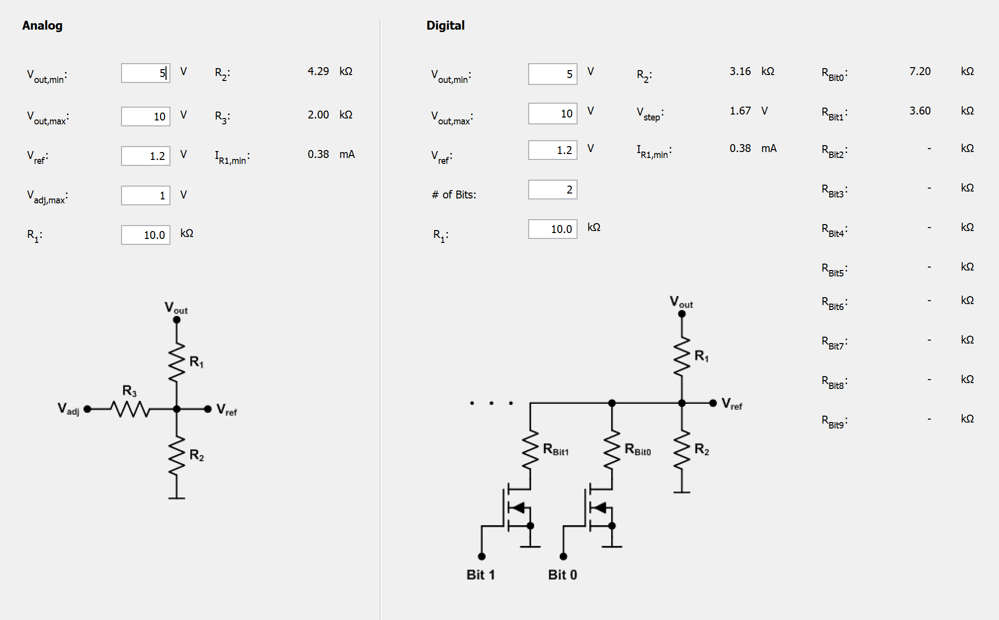
Dynamic output voltage adjustment can also be achieved by applying GPIO signals to an array of resistors and signal FET combinations in parallel with the low-side resistor of the feedback divider. For most cases, a microcontroller output in open-drain configuration can be used instead of an external signal FET because it is already part of the system. Power Stage Designer calculates the low-side feedback resistor, the voltage per step, the bias current, and the series resistance for each bit based on the output voltage range, the reference voltage, the number of bits, and the value of the high-side feedback resistor.
#T5147377-33 shows the Dynamic Output Voltage Scaling Calculator window.
 Figure 10-1 Dynamic Output Voltage Scaling
Calculator Window
Figure 10-1 Dynamic Output Voltage Scaling
Calculator WindowThe LM10011 is a device that has this feature integrated for 4/6-Bit VID.