SLVUBG9 June 2018 TPS61372
2 Schematic
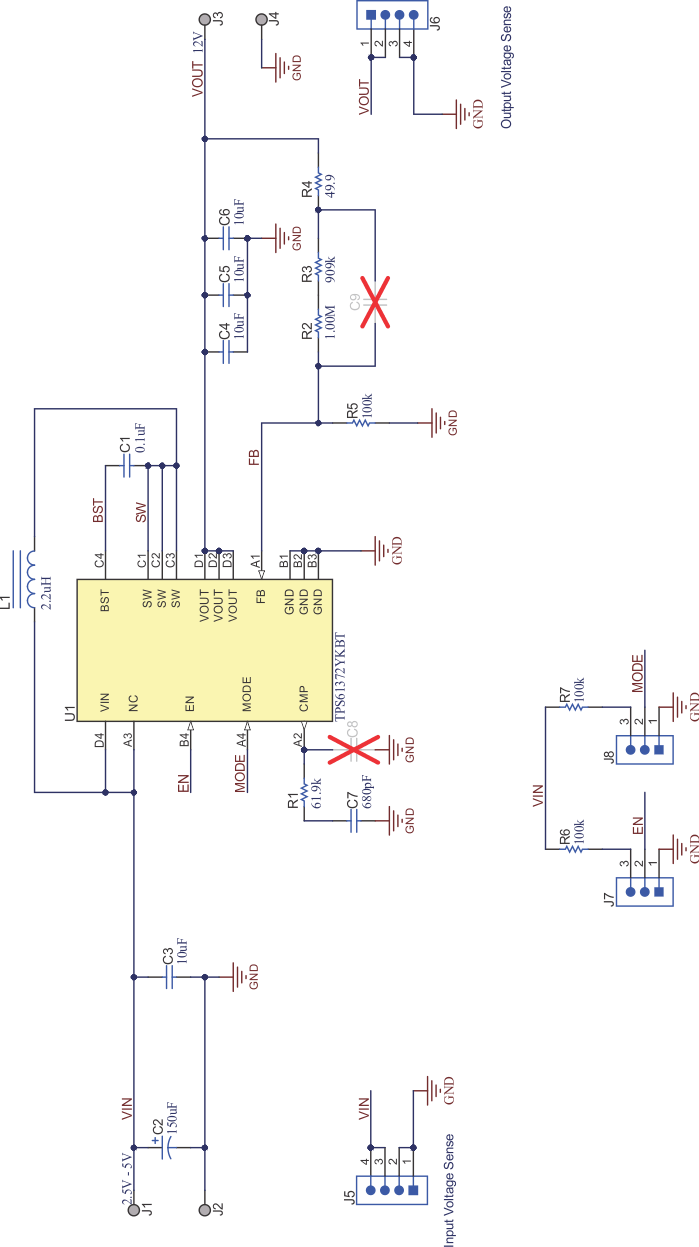
Figure 1 shows the schematic of the TPS61372EVM. Some components are used to evaluate the IC easily but unnecessary in real application, such as the 150-µF input capacitor C2, feedback resistor R4. The J5 and J6 are to detect the input and output voltages close to the IC.
The long cable between the power supply and the EVM introduces large parasitic inductance. This parasitic inductor could "ring" with the ceramic capacitor if not using a 50-mΩ ESR, 150-µF tantalum capacitor. Normally, the parasitic inductor is much smaller in real applications; so, the tantalum capacitor is not required.
The 49.9-Ω R4 is used to measure the Bode plot; this helps to estimate the stability of the boost converter while evaluating the IC. Two resistors, R2 and R3 in series, can help to precisely select the feedback divider. One resistor may be good enough for real applications.
 Figure 1. Schematic of the TPS61372EVM