SLVUBI1 May   2021


  1.   Trademarks
  2. 1TPS7H4002EVM-CVAL Overview
    1. 1.1 Features
    2. 1.2 Applications
  3. 2TPS7H4002EVM-CVAL Default Configuration
  4. 3TPS7H4002EVM-CVAL Initial Setup
  5. 4TPS7H4002EVM-CVAL Testing
    1. 4.1 Output Voltage Regulation
    2. 4.2 Output Voltage Ripple
    3. 4.3 Soft Start-up
    4. 4.4 Transient Response to Positive/Negative Load Step (0 A to 3A to 0A)
    5. 4.5 Input Voltage Ripple
    6. 4.6 Loop Frequency Response
    7. 4.7 Current Limiting
  6. 5TPS7H4002EVM-CVAL EVM Schematic
  7. 6TPS7H4002EVM-CVAL Bill of Materials (BOM)
  8. 7Board Layout

Output Voltage Regulation

  • Turn on the input DC source (5 V)
  • Turn on the e-load and sweep the load current from 0 A to 3 A, or higher to observe the margin the device has to the recommended operating condition of 3-A maximum. The monitored output voltage at TP17 (VOUT) is at or near 2.5 V across the entire current load sweep as shown in Figure 4-1.
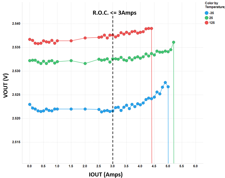
    GUID-20210517-CA0I-HKLS-CQLQ-4SRRVZ8Z2ZK1-low.png Figure 4-1 Output Voltage Regulation