SLVUBI1 May 2021
4.4 Transient Response to Positive/Negative Load Step (0 A to 3A to 0A)
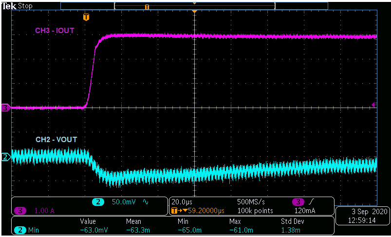
- Configure e-load to switch between 0 A and 3 A at a rate of 1 A/µs.
- On the oscilloscope, display CH2 (VOUT) [AC coupled, 50 mV/div] and CH3 (Output Current Probe) [1 A/div, trigger rising edge ≈ 120 mA] with 20 µs/div.
Figure 4-4 shows the response to this load step to be about 50mV, or 2%.
 Figure 4-4 Transient Response to Load Step 0 A to 3 A at 1 A/µs
- Change the trigger on CH3 to falling edge to capture the transient response of VOUT to negative current step from 3 A to 0 A as shown in Figure 4-5.
Again, transient deviation is approximately 50 mV, ignoring peak envelope, or 2%.
 Figure 4-5 Transient Response to Load Step 3 A to 0 A at 1 A/µs