SLVUBI2A
July 2018 – October 2020
TPS650330-Q1
,
TPS650331-Q1
Trademarks
1
Introduction
2
Requirements
3
Operation Instructions
3.1
Configuring the USB to I2C Adapter
3.2
Regulator Input Supplies and Features
3.2.1
Buck 1 Input Supply
3.2.2
Mid-Vin Buck1 Features
3.2.3
Buck 2 Input Supply
3.2.4
Buck 3 Input Supply
3.2.5
Low-Vin Buck2 and Buck3 Features
3.2.6
LDO Input Supply
3.2.7
Low Noise LDO Features
3.3
Selecting the Logic Supply Voltage
4
EVM Configurations
5
Test Points
5.1
Voltage Test Points
6
Graphical User Interface
6.1
TPS650330-Q1 EVM Debugging
6.1.1
I2C Communication Port and Adapter Debugging
6.1.2
Updating MCU Firmware
6.2
Navigating the GUI
6.2.1
Home
6.2.2
Block Diagram
6.2.3
Registers
6.2.4
Device Configuration
6.2.4.1
Using Device Configuration to Define Spin Settings
6.2.4.2
Configuring the Power Sequence
6.2.5
Re-Program PMIC
6.3
In-Circuit Programming
7
Typical Performance Plots
7.1
Power Sequence Plots
7.2
Load Transient Plots
7.3
Output Voltage Ripple Plots
7.4
Efficiency Plots
7.5
LDO Output Noise
8
TPS650330-Q1 EVM Schematic
9
TPS650330-Q1 EVM PCB Layers
10
TPS650330-Q1 EVM Bill of Materials
11
TPS650330-Q1 Silicon Revision Changes
12
Revision History
7.2
Load Transient Plots
VIN = 12 V
VOUT = 3.3 V
IOUT = 1 mA to 750 mA in 1 µs
Figure 7-3
Buck 1 Load Transient
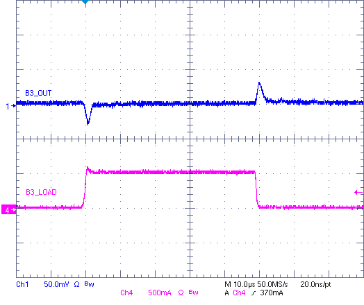
VIN = 3.3 V
VOUT = 1.2 V
IOUT = 1 mA to 300 mA in 1 µs
Figure 7-5
Buck 3 Load Transient
VIN = 3.3 V
VOUT = 1.8 V
IOUT = 1 mA to 300 mA in 1 µs
Figure 7-4
Buck 2 Load Transient