SLVUBJ0B January 2019 – June 2021 TPS56C230
4.3 Output Voltage Load Regulation
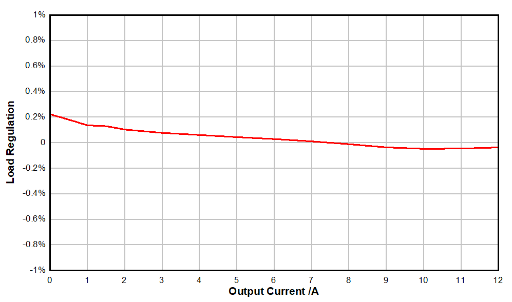
Figure 4-3 shows the load regulation for the TPS56C230EVM. Measurement is given for an ambient temperature of 25 °C.
 Figure 4-3 TPS56C230EVM Load Regulation, VIN = 12 V
SLVUBJ0B January 2019 – June 2021 TPS56C230
Figure 4-3 shows the load regulation for the TPS56C230EVM. Measurement is given for an ambient temperature of 25 °C.
 Figure 4-3 TPS56C230EVM Load Regulation, VIN = 12 V